SMB8 to SMB21: I/O Module ID and Error Registers
SMB8 through SMB21 are organized in byte pairs for expansion modules 0 to 6. As described in Table D-8, the even-numbered byte of each pair is the module-identification register. These bytes identify the module type, the I/O type, and the number of inputs and outputs. The odd-numbered byte of each pair is the module error register. These bytes provide an indication of any errors detected in the I/O for that module.
Table D-8 Special Memory Bytes SMB8 to SMB21
| SM Byte | Description (Read Only) | |
|---|---|---|
| Format | Even-Number Byte: Module ID RegisterMSB 7 LSB 0m t t a i i q qm: Module present 0 = Present1 = Not presenttt: Module type00 Non-intelligent I/O module01 Intelligent module10 Reserved11 Reserveda: I/O type 0 = Discrete1 = Analogii: Inputs00 No inputs01 2 AI or 8 DI10 4 AI or 16 DI11 8 AI or 32 DIqq: Outputs00 No outputs01 2 AQ or 8 DQ10 4 AQ or 16 DQ11 8 AQ or 32 DQ |
Odd-Number Byte: Module Error RegisterMSB 7 LSB 0c 0 0 b r p f tc: Configuration error 0 = no errorb: Bus fault or parity error 1 = errorr: Out-of-range errorp: No user power errorf: Blown fuse errort: Terminal block loose error |
| SMB8SMB9 | Module 0 ID registerModule 0 error register | |
| SMB10SMB11 | Module 1 ID registerModule 1 error register | |
| SMB12SMB13 | Module 2 ID registerModule 2 error register | |
| SMB14SMB15 | Module 3 ID registerModule 3 error register | |
| SMB16SMB17 | Module 4 ID registerModule 4 error register | |
| SMB18SMB19 | Module 5 ID registerModule 5 error register | |
| SMB20SMB21 | Module 6 ID registerModule 6 error register |
SMW22 to SMW26: Scan Times
As described in Table D-9, SMW22, SMW24, and SMW26 provide scan time information: minimum scan time, maximum scan time, and last scan time in milliseconds.
Table D-9 Special Memory Words SMW22 to SMW26
| SM Word | Description (Read Only) |
|---|---|
| SMW22 | Scan time of the last scan cycle in milliseconds |
| SMW24 | Minimum scan time in milliseconds recorded since entering the RUN mode |
| SMW26 | Maximum scan time in milliseconds recorded since entering the RUN mode |
SMB28 and SMB29: Analog Adjustment
As described in Table D-10, SMB28 holds the digital value that represents the position of analog adjustment 0. SMB29 holds the digital value that represents the position of analog adjustment 1.
Table D-10 Special Memory Bytes SMB28 and SMB29
| SM Byte | Description (Read Only) |
|---|---|
| SMB28 | This byte stores the value entered with analog adjustment 0. This value is updated once per scan in STOP/RUN. |
| SMB29 | This byte stores the value entered with analog adjustment 1. This value is updated once per scan in STOP/RUN. |
SMB30 and SMB130: Freeport Control Registers
SMB30 controls the Freeport communications for port 0; SMB130 controls the Freeport communications for port 1. You can read and write to SMB30 and SMB130. As described in Table D-11, these bytes configure the respective communications ports for Freeport operation and provide selection of either Freeport or system protocol support.
Table D-11 Special Memory Byte SMB30
| Port 0 | Port 1 | Description |
|---|---|---|
| Format of SMB30 | Format of SMB130 | Freeport mode control byteMSB 7 LSB 0┌─┬─┬─┬─┬─┬─┬─┬─┐│p│p│d│b│b│b│m│m│└─┴─┴─┴─┴─┴─┴─┴─┘ |
| SM30.0 and SM30.1 | SM130.0 and SM130.1 | mm: Protocol selection00 = Point-to-Point Interface protocol (PPI/slave mode)01 = Freeport protocol10 = PPI/master mode11 = Reserved (defaults to PPI/slave mode)Note: When you select code mm = 10 (PPI master), the S7-200 will become a master on the network and allow the NETR and NETW instructions to be executed. Bits 2 through 7 are ignored in PPI modes. |
| SM30.2 to SM30.4 | SM130.2 to SM130.4 | bbb: Freeport Baud rate000 = 38,400 baud001 = 19,200 baud010 = 9,600 baud011 = 4,800 baud100 = 2,400 baud101 = 1,200 baud110 = 115,200 baud111 = 57,600 baud |
| SM30.5 | SM130.5 | d: Data bits per character0 = 8 bits per character1 = 7 bits per character |
| SM30.6 and SM30.7 | SM130.6 and SM130.7 | pp: Parity select00 = no parity01 = even parity10 = no parity11 = odd parity |
Special Memory (SM) Bits Appendix D
SMB31 and SMW32: Permanent Memory (EEPROM) Write Control
You can save a value stored in V memory to permanent memory under the control of your program. To do this, load the address of the location to be saved in SMW32. Then, load SMB31 with the command to save the value. Once you have loaded the command to save the value, you do not change the value in V memory until the S7-200 resets SM31.7, indicating that the save operation is complete.
At the end of each scan, the S7-200 checks to see if a command to save a value to permanent memory was issued. If the command was issued, the specified value is saved to permanent memory.
As described in Table D-12, SMB31 defines the size of the data to be saved to permanent memory and provides the command that initiates a save operation. SMW32 stores the starting address in V memory for the data to be saved to permanent memory.
Table D-12 Special Memory Byte SMB31 and Special Memory Word SMW32
| SM Byte | Description |
|---|---|
| Format | SMB31: Software commandMSB 7 LSB 0c 0 0 0 0 0 s sSMW32: V memory addressMSB 15 LSB 0V memory address |
| SM31.0 and SM31.1 | ss: Size of the data00 = byte 10 = word01 = byte 11 = double word |
| SM31.7 | c: Save to permanent memory 0 = No request for a save operation to be performed1 = User program requests to save dataThe S7-200 resets this bit after each save operation. |
| SMW32 | The V memory address for the data to be saved is stored in SMW32. This value is entered as an offset from V0. When a save operation is executed, the value in this V memory address is saved to the corresponding V memory location in the permanent memory. |
SMB34 and SMB35: Time Interval Registers for Timed Interrupts
As described in Table D-13, SMB34 specifies the time interval for timed interrupt 0, and SMB35 specifies the time interval for timed interrupt 1. You can specify the time interval (in 1-ms increments) from 1 ms to 255 ms. The time-interval value is captured by the S7-200 at the time the corresponding timed interrupt event is attached to an interrupt routine. To change the time interval, you must reattach the timed interrupt event to the same or to a different interrupt routine. You can terminate the timed interrupt event by detaching the event.
Table D-13 Special Memory Bytes SMB34 and SMB35
| SM Byte | Description |
|---|---|
| SMB34 | This byte specifies the time interval (in 1-ms increments from 1 ms to 255 ms) for timed interrupt 0. |
| SMB35 | This byte specifies the time interval (in 1-ms increments from 1 ms to 255 ms) for timed interrupt 1. |
SMB36 to SMB65: HSC0, HSC1, and HSC2 Register
As described in Table D-14, SMB36 through SM65 are used to monitor and control the operation of high-speed counters HSC0, HSC1, and HSC2.
487
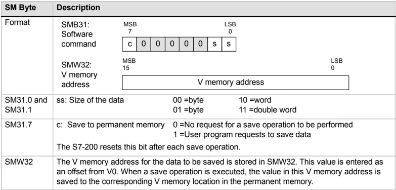
Table D-14 Special Memory Bytes SMB36 to SMD62
| SM Byte | Description |
|---|---|
| SM36.0 to SM36.4 | Reserved |
| SM36.5 | HSC0 current counting direction status bit: 1 = counting up |
| SM36.6 | HSC0 current value equals preset value status bit: 1 = equal |
| SM36.7 | HSC0 current value is greater than preset value status bit: 1 = greater than |
| SM37.0 | Active level control bit for Reset: 0= Reset is active high, 1 = Reset is active low |
| SM37.1 | Reserved |
| SM37.2 | Counting rate selection for quadrature counters:0=4x counting rate; 1=1 x counting rate |
| SM37.3 | HSC0 direction control bit: 1 = count up |
| SM37.4 | HSC0 update the direction: 1 = update direction |
| SM37.5 | HSC0 update the preset value: 1 = write new preset value to HSC0 preset |
| SM37.6 | HSC0 update the current value: 1 = write new current value to HSC0 current |
| SM37.7 | HSC0 enable bit: 1 = enable |
| SMD38 | HSC0 new current value |
| SMD42 | HSC0 new preset value |
| SM46.0 to SM46.4 | Reserved |
| SM46.5 | HSC1 current counting direction status bit: 1 = counting up |
| SM46.6 | HSC1 current value equals preset value status bit: 1 = equal |
| SM46.7 | HSC1 current value is greater than preset value status bit: 1 = greater than |
| SM47.0 | HSC1 active level control bit for reset: 0 = active high, 1 = active low |
| SM47.1 | HSC1 active level control bit for start: 0 = active high, 1 = active low |
| SM47.2 | HSC1 quadrature counter rate selection: 0 = 4x rate, 1 = 1x rate |
| SM47.3 | HSC1 direction control bit: 1 = count up |
| SM47.4 | HSC1 update the direction: 1 = update direction |
| SM47.5 | HSC1 update the preset value: 1 = write new preset value to HSC1 preset |
| SM47.6 | HSC1 update the current value: 1 = write new current value to HSC1 current |
| SM47.7 | HSC1 enable bit: 1 = enable |
| SMD48 | HSC1 new current value |
| SMD52 | HSC1 new preset value |
| SM56.0 to SM56.4 | Reserved |
| SM56.5 | HSC2 current counting direction status bit: 1 = counting up |
| SM56.6 | HSC2 current value equals preset value status bit: 1 = equal |
| SM56.7 | HSC2 current value is greater than preset value status bit: 1 = greater than |
| SM57.0 | HSC2 active level control bit for reset: 0 = active high, 1 = active low |
| SM57.1 | HSC2 active level control bit for start: 0 = active high, 1 = active low |
| SM57.2 | HSC2 quadrature counter rate selection: 0 = 4x rate, 1 = 1x rate |
| SM57.3 | HSC2 direction control bit: 1 = count up |
| SM57.4 | HSC2 update the direction: 1 = update direction |
| SM57.5 | HSC2 update the preset value: 1 = write new preset value to HSC2 preset |
| SM57.6 | HSC2 update the current value: 1 = write new current value to HSC2 current |
| SM57.7 | HSC2 enable bit: 1 = enable |
| SMD58 | HSC2 new current value |
| SMD62 | HSC2 new preset value |
488
SMB66 to SMB85: PTO/PWM Registers
As described in Table D-15, SMB66 through SMB85 are used to monitor and control the pulse train output and pulse width modulation functions. See the information on pulse output high-speed output instructions in Chapter 6 for a complete description of these bits.
Table D-15 Special Memory Bytes SMB66 to SMB85
| SM Byte | Description |
|---|---|
| SM66.0 to SM66.3 | Reserved |
| SM66.4 | PTO0 profile aborted: 0 = no error, 1 = aborted due to a delta calculation error |
| SM66.5 | PTO0 profile aborted: 0 = not aborted by user command, 1 = aborted by user command |
| SM66.6 | PTO0/PWM pipeline overflow (cleared by the system when using external profiles, otherwise must be reset by user): 0 = no overflow, 1 = pipeline overflow |
| SM66.7 | PTO0 idle bit: 0 = PTO in progress, 1 = PTO idle |
| SM67.0 | PTO0/PWM0 update the cycle time value: 1 = write new cycle time |
| SM67.1 | PWM0 update the pulse width value: 1 = write new pulse width |
| SM67.2 | PTO0 update the pulse count value: 1 = write new pulse count |
| SM67.3 | PTO0/PWM0 time base: 0 = 1 μs/tick, 1 = 1 ms/tick |
| SM67.4 | Update PWM0 synchronously: 0 = asynchronous update, 1 = synchronous update |
| SM67.5 | PTO0 operation: 0 = single segment operation (cycle time and pulse count stored in SM memory), 1 = multiple segment operation (profile table stored in V memory) |
| SM67.6 | PTO0/PWM0 mode select: 0 = PTO, 1 = PWM |
| SM67.7 | PTO0/PWM0 enable bit: 1 = enable |
| SMW68 | PTO0/PWM0 cycle time value (2 to 65,535 units of time base); |
| SMW70 | PWM0 pulse width value (0 to 65,535 units of the time base); |
| SMD72 | PTO0 pulse count value (1 to 2³² -1); |
| SM76.0 to SM76.3 | Reserved |
| SM76.4 | PTO1 profile aborted: 0 = no error, 1 = aborted because of delta calculation error |
| SM76.5 | PTO1 profile aborted: 0 = not aborted by user command, 1 = aborted by user command |
| SM76.6 | PTO1/PWM pipeline overflow (cleared by the system when using external profiles, otherwise must be reset by the user): 0 = no overflow, 1 = pipeline overflow |
| SM76.7 | PTO1 idle bit: 0 = PTO in progress, 1 = PTO idle |
| SM77.0 | PTO1/PWM1 update the cycle time value: 1 = write new cycle time |
| SM77.1 | PWM1 update the pulse width value: 1 = write new pulse width |
| SM77.2 | PTO1 update the pulse count value: 1 = write new pulse count |
| SM77.3 | PTO1/PWM1 time base: 0 = 1 μs/tick, 1 = 1 ms/tick |
| SM77.4 | Update PWM1 synchronously: 0 = asynchronous update, 1 = synchronous update |
| SM77.5 | PTO1 operation: 0 = single segment operation (cycle time and pulse count stored in SM memory), 1 = multiple segment operation (profile table stored in V memory) |
| SM77.6 | PTO1/PWM1 mode select: 0 = PTO, 1 = PWM |
| SM77.7 | PTO1/PWM1 enable bit: 1 = enable |
| SMW78 | PTO1/PWM1 cycle time value (2 to 65,535 units of the time base); |
| SMW80 | PWM1 pulse width value (0 to 65,535 units of the time base); |
| SMD82 | PTO1 pulse count value (1 to 2³² -1); |
SMB86 to SMB94, and SMB186 to SMB194: Receive Message Control
As described in Table D-16, SMB86 through SMB94 and SMB186 through SMB194 are used to control and read the status of the Receive Message instruction.
Table D-16 Special Memory Bytes SMB86 to SMB94, and SMB186 to SMB194
| Port 0 | Port 1 | Description |
|---|---|---|
| SMB86 | SMB186 | Receive Message status byteMSB 7LSB 0<br>n r e 0 0 t c p<br>n: 1 = Receive message terminated by user disable commandr: 1 = Receive message terminated: error in input parameters or missing start or end conditione: 1 = End character receivedt: 1 = Receive message terminated: timer expiredc: 1 = Receive message terminated: maximum character count achievedp 1 = Receive message terminated because of a parity error |
| SMB87 | SMB187 | Receive Message control byteMSB 7LSB 0<br>en sc ec il c/m tmr bk 0<br>en: 0 = Receive Message function is disabled.1 = Receive Message function is enabled.The enable/disable receive message bit is checked each time the RCV instruction is executed.sc: 0 = Ignore SMB88 or SMB188.1 = Use the value of SMB88 or SMB188 to detect start of message.ec: 0 = Ignore SMB89 or SMB189.1 = Use the value of SMB89 or SMB189 to detect end of message.il: 0 = Ignore SMW90 or SMW190.1 = Use the value of SMW90 or SMW190 to detect an idle line condition.c/m: 0 = Timer is an inter-character timer.1 = Timer is a message timer.tmr: 0 = Ignore SMW92 or SMW192.1 = Terminate receive if the time period in SMW92 or SMW192 is exceeded.bk: 0 = Ignore break conditions.1 = Use break condition as start of message detection. |
| SMB88 | SMB188 | Start of message character |
| SMB89 | SMB189 | End of message character |
| SMW90 | SMW190 | Idle line time period given in milliseconds. The first character received after idle line time has expired is the start of a new message. |
| SMW92 | SMW192 | Inter-character/message timer time-out value (in milliseconds). If the time period is exceeded, the receive message is terminated. |
| SMB94 | SMB194 | Maximum number of characters to be received (1 to 255 bytes).Note: This range must be set to the expected maximum buffer size, even if the character count message termination is not used. |
Special Memory (SM) Bits Appendix D
SMW98: Errors on the Expansion I/O Bus
As described in Table D-17, SMW98 gives you information about the number of errors on the expansion I/O bus.
Table D-17 Special Memory Bytes SMW98
| SM Byte | Description |
|---|---|
| SMW98 | This location is incremented each time a parity error is detected on the expansion I/O bus. It is cleared upon power up, and can be cleared by the user. |
SMB130: Freeport Control Register (see SMB30)
Refer to Table D-11.
SMB131 to SMB165: HSC3, HSC4, and HSC5 Register
As described in Table D-18, SMB131 through SMB165 are used to monitor and control the operation of high-speed counters HSC3, HSC4, and HSC5.
Table D-18 Special Memory Bytes SMB131 to SMB165
| SM Byte | Description |
|---|---|
| SMB131 to SMB135 | Reserved |
| SM136.0 to SM136.4 | Reserved |
| SM136.5 | HSC3 current counting direction status bit: 1 = counting up |
| SM136.6 | HSC3 current value equals preset value status bit: 1 = equal |
| SM136.7 | HSC3 current value is greater than preset value status bit: 1 = greater than |
| SM137.0 to SM137.2 | Reserved |
| SM137.3 | HSC3 direction control bit: 1 = count up |
| SM137.4 | HSC3 update direction: 1 = update direction |
| SM137.5 | HSC3 update preset value: 1 = write new preset value to HSC3 preset |
| SM137.6 | HSC3 update current value: 1 = write new current value to HSC3 current |
| SM137.7 | HSC3 enable bit: 1 = enable |
| SMD138 | HSC3 new current value |
| SMD142 | HSC3 new preset value |
| SM146.0 to SM146.4 | Reserved |
| SM146.5 | HSC4 current counting direction status bit: 1 = counting up |
| SM146.6 | HSC4 current value equals preset value status bit: 1 = equal |
| SM146.7 | HSC4 current value is greater than preset value status bit: 1 = greater than |
| SM147.0 | Active level control bit for Reset: 0 = Reset is active high, 1 = Reset is active low |
| SM147.1 | Reserved |
| SM147.2 | Counting rate selection for quadrature counters: 0 = 4x counting rate, 1 = 1x counting rate |
| SM147.3 | HSC4 direction control bit: 1 = count up |
| SM147.4 | HSC4 update direction: 1 = update direction |
| SM147.5 | HSC4 update preset value: 1 = write new preset value to HSC4 preset |
| SM147.6 | HSC4 update current value: 1 = write new current value to HSC4 current |
| SM147.7 | HSC4 enable bit: 1 = enable |
| SMD148 | HSC4 new current value |
| SMD152 | HSC4 new preset value |
| SM156.0 to SM156.4 | Reserved |
491
Table D-18 Special Memory Bytes SMB131 to SMB165, continued
| SM Byte | Description |
|---|---|
| SM156.5 | HSC5 current counting direction status bit: 1 = counting up |
| SM156.6 | HSC5 current value equals preset value status bit: 1 = equal |
| SM156.7 | HSC5 current value is greater than preset value status bit: 1 = greater than |
| SM157.0 to SM157.2 | Reserved |
| SM157.3 | HSC5 direction control bit: 1 = count up |
| SM157.4 | HSC5 update direction: 1 = update direction |
| SM157.5 | HSC5 update preset value: 1 = write new preset value to HSC5 preset |
| SM157.6 | HSC5 update current value: 1 = write new current value to HSC5 current |
| SM157.7 | HSC5 enable bit: 1 = enable |
| SMD158 | HSC5 new current value |
| SMD162 | HSC5 new preset value |
SMB166 to SMB185: PTO0, PTO1 Profile Definition Table
As described in Table D-19, SMB166 through SMB185 are used to show the number of active profile steps and the address of the profile table in V memory.
Table D-19 Special Memory Bytes SMB166 to SMB185
| SM Byte | Description |
|---|---|
| SMB166 | Current entry number of the active profile step for PTO0 |
| SMB167 | Reserved |
| SMW168 | V memory address of the profile table for PTO0 given as an offset from V0. |
| SMB170 | Linear PTO0 status byte |
| SMB171 | Linear PTO0 result byte |
| SMD172 | Specifies the frequency to be generated when the Linear PTO0 generator is operated in manual mode. The frequency is specified as a double integer value in Hz. SMB172 is MSB and SMB175 is LSB |
| SMB176 | Current entry number of the active profile step for PTO1 |
| SMB177 | Reserved |
| SMW178 | V memory address of the profile table for PTO1 given as an offset from V0. |
| SMB180 | Linear PTO1 status byte |
| SMB181 | Linear PTO1 result byte |
| SMD182 | Specifies the frequency to be generated when the Linear PTO1 generator is operated in manual mode. The frequency is specified as a double integer value in Hz. SMB182 is MSB and SMB178 is LSB |
SMB186 to SMB194: Receive Message Control (see SMB86 to SMB94)
Refer to Table D-16.
492
SMB200 to SMB549: Intelligent Module Status
As shown in Table D-20, SMB200 through SMB549 are reserved for information provided by intelligent expansion modules, such as the EM 277 PROFIBUS-DP module. For information about how your module uses SMB200 through SMB549, refer to Appendix A for the specifications of your specific module.
For an S7-200 CPU with firmware prior to version 1.2, you must install the intelligent module next to the CPU in order to ensure compatibility.
Table D-20 Special Memory Bytes SMB200 to SMB549
| Intelligent Module in Slot 0 | Intelligent Module in Slot 1 | Intelligent Module in Slot 2 | Intelligent Module in Slot 3 | Intelligent Module in Slot 4 | Intelligent Module in Slot 5 | Intelligent Module in Slot 6 | Description |
|---|---|---|---|---|---|---|---|
| SMB200 to SMB215 | SMB250 to SMB265 | SMB300 to SMB315 | SMB350 to SMB365 | SMB400 to SMB415 | SMB450 to SMB465 | SMB500 to SMB515 | Module name (16 ASCII characters) |
| SMB216 to SMB219 | SMB266 to SMB269 | SMB316 to SMB319 | SMB366 to SMB369 | SMB416 to SMB419 | SMB466 to SMB469 | SMB516 to SMB519 | S/W revision number (4 ASCII characters) |
| SMW220 | SMW270 | SMW320 | SMW370 | SMW420 | SMW470 | SMW520 | Error code |
| SMB222 to SMB249 | SMB272 to SMB299 | SMB322 to SMB349 | SMB372 to SMB399 | SMB422 to SMB449 | SMB472 to SMB499 | SMB522 to SMB549 | Information specific to the particular module type |
SIMATIC S7-200 Order Numbers
CPUs
| Description | Order Number |
|---|---|
| CPU 221 DC/DC/DC 6 Inputs/4 Outputs | 6ES7 211-0AA23-0XB0 |
| CPU 221 AC/DC/Relay 6 Inputs/4 Relays | 6ES7 211-0BA23-0XB0 |
| CPU 222 DC/DC/DC 8 Inputs/6 Outputs | 6ES7 212-1AB23-0XB0 |
| CPU 222 AC/DC/Relay 8 Inputs/6 Relays | 6ES7 212-1BB23-0XB0 |
| CPU 224 DC/DC/DC 14 Inputs/10 Outputs | 6ES7 214-1AD23-0XB0 |
| CPU 224 AC/DC/Relay 14 Inputs/10 Relays | 6ES7 214-1BD23-0XB0 |
| CPU 224XP DC/DC/DC 14 Inputs/10 Outputs | 6ES7 214-2AD23-0XB0 |
| CPU 224XP AC/DC/Relay 14 Inputs/10 Relays | 6ES7 214-2BD23-0XB0 |
| CPU 224XPsi DC/DC/DC 14 Inputs/10 Outputs | 6ES7 214-2AS23-0XB0 |
| CPU 226 DC/DC/DC 24 Inputs/16 Outputs | 6ES7 216-2AD23-0XB0 |
| CPU 226 AC/DC/Relay 24 Inputs/16 Relays | 6ES7 216-2BD23-0XB0 |
Expansion Modules
| Description | Order Number |
|---|---|
| EM 221 24 VDC Digital 8 Inputs | 6ES7 221-1BF22-0XA0 |
| EM 221 Digital 8 AC Inputs (8 x 120/230 VAC) | 6ES7 221-1EF22-0XA0 |
| EM 221 Digital Input 16 x 24 VDC | 6ES7 221-1BH22-0XA0 |
| EM 222 24 VDC Digital 8 Outputs | 6ES7 222-1BF22-0XA0 |
| EM 222 Digital Output 8 x Relay | 6ES7 222-1HF22-0XA0 |
| EM 222 Digital 8 AC Outputs (8 x 120/230 VAC) | 6ES7 222-1EF22-0XA0 |
| EM 222 Digital Output 4 x 24 VDC - 5A | 6ES7 222-1BD22-0XA0 |
| EM 222 Digital Output 4 x Relays -10A | 6ES7 222-1HD22-0XA0 |
| EM 223 24 VDC Digital Combination 4 Inputs/4 Outputs | 6ES7 223-1BF22-0XA0 |
| EM 223 24 VDC Digital Combination 4 Inputs/4 Relay Outputs | 6ES7 223-1HF22-0XA0 |
| EM 223 24 VDC Digital Combination 8 Inputs/8 Outputs | 6ES7 223-1BH22-0XA0 |
| EM 223 24 VDC Digital Combination 8 Inputs/8 Relay Outputs | 6ES7 223-1PH22-0XA0 |
| EM 223 24 VDC Digital Combination 16 Inputs/16 Outputs | 6ES7 223-1BL22-0XA0 |
| EM 223 24 VDC Digital Combination 16 Inputs/16 Relay Outputs | 6ES7 223-1PL22-0XA0 |
| EM 223 24 VDC Digital Combination 32 Inputs/32 Outputs | 6ES7 223-1BM22-0XA0 |
| EM 223 24 VDC Digital Combination 32 Inputs/32 Relay Outputs | 6ES7 223-1PM22-0XA0 |
| EM 231 Analog Input, 4 Inputs | 6ES7 231-0HC22-0XA0 |
| EM 231 Analog Input, 8 Inputs | 6ES7 231-0HF22-0XA0 |
| EM 231 Analog Input RTD, 2 Inputs | 6ES7 231-7PB22-0XA0 |
| EM 231 Analog Input RTD, 4 Inputs | 6ES7 231-7PC22-0XA0 |
| EM 231 Analog Input Thermocouple, 4 Inputs | 6ES7 231-7PD22-0XA0 |
| EM 231 Analog Input Thermocouple, 8 Inputs | 6ES7 231-7PF22-0XA0 |
| EM 232 Analog Output, 2 Outputs | 6ES7 232-0HB22-0XA0 |
| EM 232 Analog Output, 4 Outputs | 6ES7 232-0HD22-0XA0 |
| EM 235 Analog Combination 4 Inputs/1 Output | 6ES7 235-0KD22-0XA0 |
| EM 241 Modem Module | 6ES7 241-1AA22-0XA0 |
| EM 253 Position Module | 6ES7 253-1AA22-0XA0 |
495

| Expansion Modules | Order Number |
|---|---|
| SIWAREX MS Micro Scale Module (includes manual) | 7MH4 930-0AA01 |
| SINAUT MD720-3 GSM/GPRS Modem | 6NH9 720-3AA00 |
| SINAUT ANT 794-4MR Antenna GSM Quadband AMD UMTS | 6NH9 860-1AA00 |
| Communications Modules | Order Number |
|---|---|
| EM 277 PROFIBUS-DP Module | 6ES7 277-0AA22-0XA0 |
| CP 243-2 AS Interface Module | 6GK7 243-2AX01-0XA0 |
| CP 243-1 Ethernet Module (with electronic documentation on CD) | 6GK7 243-1EX00-0XE0 |
| CP 243-1 IT Internet Module (with electronic documentation on CD) | 6GK7 243-1GX00-0XE0 |
| Cartridges and Cables | Order Number |
|---|---|
| Memory Cartridge, 64K (user program, recipe, and data logging) | 6ES7 291-8GF23-0XA0 |
| Memory Cartridge, 256K (user program, recipe, and data logging) | 6ES7 291-8GH23-0XA0 |
| Real-Time Clock with battery Cartridge (CPU 221 and CPU 222) | 6ES7 297-1AA23-0XA0 |
| Battery Cartridge | 6ES7 291-8BA20-0XA0 |
| I/O Bus Extension Cable, 0.8 meters | 6ES7 290-6AA20-0XA0 |
| Programming Cable, RS-232/PPI Multi-Master | 6ES7 901-3CB30-0XA0 |
| Programming Cable, USB/PPI Multi-Master | 6ES7 901-3DB30-0XA0 |
| P/C Adapter, USB | 6ES7 972-0CB20-0XA0 |
| SIWAREX MS - SIWATOOL MS Cable | 7MH4 702-8CB |
| Software | Order Number |
|---|---|
| STEP 7-Micro/WIN (V4.0) Individual License (CD-ROM) | 6ES7 810-2CC03-0YX0 |
| STEP 7-Micro/WIN (V4.0) Upgrade License (CD-ROM) | 6ES7 810-2CC03-0YX3 |
| STEP 7-Micro/WIN Add-on: STEP 7-Micro/WIN 32 Instruction Library, V1.1 (CD-ROM) | 6ES7 830-2BC00-0YX0 |
| S7-200 PC Access V1.0 (OPC Server) Individual License | 6ES7 840-2CC01-0YX0 |
| S7-200 PC Access V1.0 (OPC Server) Multi-copy License | 6ES7 840-2CC01-0YX1 |
| WinCC flexible 2007 Micro Individual License (DVD-ROM without license key) | 6AV6 610-0AA01-2CA8 |
| WinCC flexible 2007 Micro Upgrade License (DVD-ROM without license key) | 6AV6 610-0AA01-2CE8 |
| WinCC flexible 2007 Compact Individual License (DVD-ROM with license key) | 6AV6 611-0AA51-2CA5 |
| WinCC flexible 2007 Compact Upgrade License (DVD-ROM with license key) | 6AV6 611-0AA51-2CE5 |
| SIWATOOL MS Configuration software or SIWAREX MS Micro Scale | 7MH4 930-0AK01 |
| SINAUT MICRO SC 8 Single License for 1 Installation | 6NH9 910-0AA10-0AA3 |
| SINAUT MICRO SC 64 Single License for 1 Installation | 6NH9 910-0AA10-0AA6 |
| SINAUT MICRO SC 256 Single License for 1 Installation | 6NH9 910-0AA10-0AA8 |
| Communications Cards | Order Number |
|---|---|
| CP 5411: Short AT ISA | 6GK1 541-1AA00 |
| CP 5512: PCMCIA Type II | 6GK1 551-2AA00 |
| CP 5611: PCI card (version 3.0 or greater) | 6GK1 561-1AA00 |
496
SIMATIC S7-200 Order Numbers Appendix E
| Manuals | Order Number |
|---|---|
| S7-200 Programmable Controller System Manual (German) | 6ES7 298-8FA24-8AH0 |
| S7-200 Programmable Controller System Manual (English) | 6ES7 298-8FA24-8BH0 |
| S7-200 Programmable Controller System Manual (French) | 6ES7 298-8FA24-8CH0 |
| S7-200 Programmable Controller System Manual (Spanish) | 6ES7 298-8FA24-8DH0 |
| S7-200 Programmable Controller System Manual (Italian) | 6ES7 298-8FA24-8EH0 |
| S7-200 Programmable Controller System Manual (Chinese) | 6ES7 298-8FA24-8FH0 |
| S7-200 Programmable Controller System Manual (Korean) | 6ES7 298-8FA24-8GH0 |
| S7-200 Point-to-Point Interface Communication Manual (English/German) | 6ES7 298-8GA00-8XH0 |
| CP 243-2 AS-Interface Master Manual (English) | 6GK7 243-2AX00-8BA0 |
| OP 73micro and TP 177micro User Manual (English) | 6AV6 691-1DF01-0AB0 |
| WinCC flexible 2005 Micro User's Manual | 6AV6 691-1AA01-0AB0 |
| SIMATIC HMI Manual Collection | 6AV6 691-1SA01-0AX0 |
| Cables, Network Connectors, and Repeaters | Order Number |
|---|---|
| MPI Cable | 6ES7 901-0BF00-0AA0 |
| PROFIBUS Network Cable | 6XV1 830-0AH10 |
| Network Bus Connector with Programming Port Connector, Vertical Cable Outlet | 6ES7 972-0BB11-0XA0 |
| Network Bus Connector (no programming port connector), Vertical Cable Outlet | 6ES7 972-0BA11-0XA0 |
| RS-485 Bus Connector with 35° Cable Outlet (no programming port connector) | 6ES7 972-0BA40-0XA0 |
| RS-485 Bus Connector with 35° Cable Outlet (with programming port connector) | 6ES7 972-0BB40-0XA0 |
| Terminal Block (7 position) | 6ES7 292-1AD20-0AA0 |
| Terminal Block (12 position) | 6ES7 292-1AE20-0AA0 |
| Terminal Block (14 position) | 6ES7 292-1AF20-0AA0 |
| Terminal Block (18 position) | 6ES7 292-1AG20-0AA0 |
| RS-485 IP 20 Repeater, Isolated | 6ES7 972-0AA00-0XA0 |
| TD/CPU Connecting Cable | 6ES7 901-3EB10-0XA0 |
| Human Machine Interface | Order Number |
|---|---|
| TD 100C Operator Interface¹ | 6ES7 272-1BA10-0YA1 |
| TD 200 Operator Interface | 6ES7 272-0AA30-0YA1 |
| TD 200C Operator Interface¹ | 6ES7 272-1AA10-0YA1 |
| TD400C Operator Interface¹ | 6AV6 640-0AA00-0AX1 |
| TD 100C Blank faceplate material, A4 size (10 sheets/package) | 6ES7 272-1BF00-7AA0 |
| TD 200C Blank faceplate material, A4 size (10 sheets/package) | 6ES7 272-1AF00-7AA0 |
| TD400C Blank faceplate material, A4 size (10 sheets/package) | 6AV6 671-0AP00-0AX0 |
| OP 73micro Operator Panel | 6AV6 640-0BA11-0AX0 |
| TP177micro Touch Panel | 6AV6 640-0CA11-0AX0 |
| Miscellaneous | Order Number |
|---|---|
| 12-Position Fan Out Connector of CPU 221 and CPU 222 (package of 10) | 6ES7 290-2AA00-0XA0 |
| Front Door Spare Part Kit for 22x CPU and EM, (4 pieces of each type) | 6ES7 291-3AX20-0XA0 |
| Simulator Module, 8 DI Switches, DC Input, for CPU 221 and 222 | 6ES7 274 1XF00-0XA0 |
| Simulator Module, 14 DI Switches, DC Input, for CPU 224 and 224XP | 6ES7 274 1XH00-0XA0 |
| Simulator Module, 24 DI Switches, DC Input, for CPU 226 | 6ES7 274 1XK00-0XA0 |
¹ Includes one blank faceplate overlay for customization. For additional blank faceplate overlays, order the blank faceplate material for your TD device.
497
Execution Times for STL Instructions
Instruction execution times are very important if your application has time-critical functions. The instruction execution times are shown in Table F-2.
Tip When you use the execution times in Table F-2, you should consider the effect of power flow to the instruction, the effect of indirect addressing, and the use of certain memory areas on these execution times. These factors can directly effect the listed execution times.
Effect of Power Flow
Table F-2 shows the time required for executing the logic or function of the instruction when power flow is present (Top of Stack = 1 or ON) for that instruction.
When power flow is not present, then the execution time for that instruction is 1 µs.
Effect of Indirect Addressing
Table F-2 shows the time required for executing the logic, or function, of the instruction when you use direct addressing of the operands and constants.
When instructions use indirectly addressed operands, the execution time for the instruction increases by 14 µs for each indirectly addressed operand used in the instruction.
Effect of Accessing Certain Memory Areas
Accessing certain memory areas, such as AI, AQ, L, and accumulators require additional execution time.
Table F-1 shows the additional time that must be added to an instruction's execution time when these memory areas are specified in an operand.
Table F-1 Adder for Accessing Memory Areas
Table F-2 Instruction Execution Times
| Instruction | µS |
|---|---|
| = Using: I | 0.24 |
| S M, T, C, V, S, Q, M | 1.3 |
| L | 10.5 |
| +D | 29 |
| -D | 29 |
| *D | 47 |
| /D | 250 |
| +I | 25 |
| -I | 25 |
| *I | 37 |
| /I | 64 |
| =I Using: Local outputs | 16 |
| Expansion outputs | 24 |
| +R | 71 Typ |
| 99 Max | |
| -R | 72 Typ |
| 100 Max | |
| *R | 56 Typ |
| 166 Max | |
| /R | 177 Typ |
| 230 Max | |
| A Using: I | 0.22 |
| S M, T, C, V, S, Q, M | 0.72 |
| L | 6.1 |
| AB <=, =, >=, >, <, <> | 18 |
| AD <=, =, >=, >, <, <> | 27 |
| AENO | 0.4 |
| AI Using: Local inputs | 15 |
| Expansion inputs | 21 |
| ALD | 0.22 |
| AN Using: I | 0.22 |
| S M, T, C, V, S, Q, M | 0.72 |
| L | 6.1 |
| ANDB | 19 |
| ANDD | 30 |
| ANDW | 25 |
| ANI Using: Local inputs | 15 |
| Expansion inputs | 21 |
| AR <=, =, >=, >, <, <> | 29 |
| AS=, <> Time = Base + (LM * N) | |
| Base | 33 |
| Length multiplier (LM) | 6.3 |
| N is the number of characters compared | |
| ATCH | 12 |
| ATH Time = Base + (length * LM) | |
| Base (constant length) | 23 |
| Base (variable length) | 31 |
| Length multiplier (LM) | 10.2 |
| ATT | 36 |
| AW <=, =, >=, >, <, <> | 23 |
| BCDI | 35 |
| Instruction | µS |
|---|---|
| BITIM | 16 |
| BIR Using: Local inputs | 23 |
| Expansion inputs | 30 |
| BIW Using: Local outputs | 24 |
| Expansion outputs | 32 |
| BMB Time = Base + (length * LM) | |
| Base (constant length) | 10 |
| Base (variable length) | 28 |
| Length multiplier (LM) | 5.7 |
| BMD Time= Base + (length * LM) | |
| Base (constant length) | 11 |
| Base (variable length) | 29 |
| Length multiplier (LM) | 10.6 |
| BMW Time= Base + (length * LM) | |
| Base (constant length) | 10 |
| Base (variable length) | 28 |
| Length multiplier (LM) | 8.6 |
| BTI | 16 |
| CALL Using no parameters: | 9 |
| Using parameters: | |
| Time = Base + Σ (operand time) | 14 |
| Base | |
| Operand time | |
| bit (input, output) | 10, 11 |
| byte (input, output) | 8, 7 |
| word (input, output) | 10, 9 |
| Dword (input, output) | 12, 10 |
| Note: processing of output operands occurs during the return from the subroutine | |
| CEVNT | 24 |
| CFND Maximum Time = Base + N1 * ((LM1 * N2) + LM2) | |
| Base | 35 |
| Length multiplier 1 (LM1) | 8.6 |
| Length multiplier 2 (LM2) | 9.5 |
| N1 is length of the source string | |
| N2 is the length of the character set string | |
| CITIM | 23 |
| COS | 900 Typ |
| 1070 Max | |
| CRET Power flow present | 16 |
| Power flow not present | 0.8 |
| CRETI Power flow not present | 0.2 |
| CSCRE | 3.1 |
| CTD On transition of count input | 27 |
| Otherwise | 19 |
| CTU On transition of count input | 31 |
| Otherwise | 19 |
| CTUD On transition of count input | 37 |
| Otherwise | 24 |
| DECB | 16 |
| DECD | 22 |
| DECO | 19 |
| DECW | 20 |
| DISI | 9 |
| DIV | 67 |
500
Execution Times for STL Instructions Appendix F
| Instruction | µS |
|---|---|
| DLED | 14 |
| DTA | 302 |
| DTI | 21 |
| DTCH | 12 |
| DTR | 35 Typ40 Max |
| DTS | 305 |
| ED | 8 |
| ENCO | 24 Max |
| END | Power flow not present0.2 |
| ENI | 11 |
| EU | 8 |
| EXP | 720 Typ860 Max |
| FIFO | Time = Base + (length * LM)BaseLength multiplier (LM)307 |
| FILL | Time= Base + (length * LM)Base (constant length)Base (variable length)Length multiplier (LM)15293.2 |
| FND <, =, >, <> | Time = Base+(length * LM)BaseLength multiplier (LM)396.5 |
| FOR | Time = Base+(Number of loops * LM)BaseLoop multiplier (LM)3528 |
| GPA | 16 |
| HDEF | 18 |
| HSC | 30 |
| HTA | Time= Base+ (length * LM)Base (constant length)Base (variable length)Length multiplier (LM)20285.2 |
| IBCD | 52 |
| INCB | 15 |
| INCD | 22 |
| INCW | 20 |
| INT | Typical with 1 interrupt24 |
| INVB | 16 |
| INVD | 22 |
| INVW | 20 |
| ITA | 136 |
| ITB | 17 |
| ITD | 20 |
| ITS | 139 |
| JMP | 1.8 |
| LBL | 0.22 |
| Instruction | µS |
|---|---|
| LD | Using: ISM, T, C, V, S, Q, ML0.220.86 |
| LDB <=, =, >=, >, <, <> | 18 |
| LDD <=, =, >=, >, <, <> | 27 |
| LDI | Using: Local inputsExpansion inputs1521 |
| LDN | Using: ISM, T, C, V, S, Q, ML0.30.96.1 |
| LDNI | Using: Local inputsExpansion inputs1521 |
| LDR <=, =, >=, >, <, <> | 29 |
| LDS | 0.22 |
| LDS=, <> | Time = Base + (LM * N)BaseLength multiplier (LM)N is the number of characters compared336.3 |
| LDW <=, =, >=, >, <, <> | 24 |
| LIFO | 37 |
| LN | 680 Typ820 Max |
| LPP | 0.22 |
| LPS | 0.24 |
| LRD | 0.22 |
| LSCR | 7.3 |
| MOVB | 15 |
| MOVD | 20 |
| MOVR | 20 |
| MOVW | 18 |
| MUL | 37 |
| NETR | 99 |
| NETW | Time = Base + (LM * N)BaseLength multiplier (LM)N is the number of bytes to send954 |
| NEXT | 0 |
| NOP | 0.22 |
| NOT | 0.22 |
| O | Using: ISM, T, C, V, S, Q, ML0.220.726.4 |
| OB <=, =, >=, >, <, <> | 18 |
| OD <=, =, >=, >, <, <> | 26 |
| OI | Using: Local inputsExpansion inputs1521 |
| OLD | 0.22 |
| ON | Using: ISM, T, C, V, S, Q, ML0.220.726.4 |
501
| Instruction | µS |
|---|---|
| ONI Using: Local inputs Expansion inputs | 15 21 |
| OR <=, =, >=, >, <, <> | 29 |
| ORB | 19 |
| ORD | 29 |
| ORW | 25 |
| OS=, < > Time + Base + (LM * N) Base Length multiplier (LM) N is the number of characters compared | 33 6.3 |
| OW <=, =, >=, >, <, <> | 24 |
| PID Typical Manual-to-auto transition Coefficient recalculation Auto-tune | 400 800 Max 770 Max 650 Max |
| PLS: Using: PWM PTO single segment PTO multiple segment | 31 36 50 |
| R Length=1 and specified as a constant Base for Counters (C) Base for Timers (T) Base for all others Otherwise: Time = Base + (length * LM) Base for Counters Base for Timers (T) Base for all others Length multiplier (LM) for operand C Length multiplier (LM) for operand T Length multiplier (LM) for all others If length stored as variable, add to base | 9.3 16 2.9 8.6 8.3 14 5.1 9.9 0.5 17 |
| RCV | 51 |
| RET | 16 |
| RI Time = Base + (length * LM) Base Length multiplier (LM) using local outputs Length multiplier (LM) using expansion outputs If length stored as a variable, add to Base | 8.9 13 21 17 |
| RLB Time = Base + (LM * N) Base Length multiplier (LM) N is the shift count | 23 0.2 |
| RLD Time = Base + (LM * N) Base Length multiplier (LM) N is the shift count | 28 1.4 |
| RLW Time = Base + (LM * N) Base Length multiplier (LM) N is the shift count | 27 0.9 |
| ROUND | 56 Typ 110 Max |
| RRB Time = Base + (LM * N) Base Length multiplier (LM) N is the shift count | 22 0.5 |
| RRD Time = Base + (LM * N) Base Length multiplier (LM)) N is the shift count | 28 1.7 |
| Instruction | µS |
|---|---|
| RRW Time = Base + (LM * N) Base Length multiplier (LM) N is the shift count | 26 1.2 |
| RTA Time = Base + (LM * N) Base (for first digit in result) Length multiplier (LM) N is the number of additional digits in result | 149 96 |
| RTS Time = Base + (LM * N) Base (for first digit in result x) Length multiplier (LM) N is the number of additional digits in result | 154 96 |
| S For length = 1 and specified as a constant Otherwise: Time = Base + (length * LM) Base Length multiplier (LM) If length is stored as a variable, add to Base | 2.9 14 0.5 17 |
| SCAT Time = Base + (LM * N) Base Length multiplier (LM) N is the number of appended characters | 30 5.3 |
| SC PY Time = Base + (LM * N) Base Length multiplier (LM) N is the number of copied characters | 27 4.6 |
| SCRE | 0.24 |
| SCRT | 10 |
| SEG | 15 |
| SFND Maximum Time = Base +((N1-N2) * LM2) +(N2 * LM1) Base Length multiplier 1 (LM1) Length multiplier 2 (LM2) N1 is the length of the source string N2 is the length of the search string | 39 7.6 6.8 |
| SHRB Time = Base + (length * LM1) + ((length /8) * LM2) Base (constant length) Base (variable length) Length multiplier 1 (LM1) Length multiplier 2 (LM2) | 48 52 1.0 1.5 |
| SI Time = Base + (length * LM) Base LM using local output LM using expansion output If length is stored as a variable, add to Base | 8.9 13 21 17 |
| SIN | 900 Typ 1070 Max |
| SLB Time = Base + (LM * N) Base Length multiplier (LM) N is the shift count | 23 0.2 |
| SLD Time = Base + (LM * N) Base Length multiplier (LM) N is the shift count | 29 1.1 |
502
Execution Times for STL Instructions Appendix F
| Instruction | µS |
|---|---|
| SLEN | 21 |
| SLW Time = Base + (LM + N) Base Length multiplier (LM)) N is the shift count | 27 0.6 |
| SPA | 371 |
| SQRT | 460 Typ 550 Max |
| SRB Time = Base + (LM + N) Base Length multiplier (LM)) N is the shift count | 22 0.6 |
| SRD Time = Base + (LM + N) Base Length multiplier (LM)) N is the shift count | 28 1.5 |
| SRW Time = Base + (LM + N) Base Length multiplier (LM)) N is the shift count | 27 1 |
| SSCPY Time = Base + (LM * N) Base Length multiplier (LM) N is the number of copied characters | 42 5.3 |
| STD Time = Base + (LM * N) Base (for 1st source character) Length multiplier (LM) N is the number of additional source characters | 69 27 |
| STI Time = Base + (LM * N) Base (for 1st source character) Length multiplier (LM) N is the number of additional source characters | 58 27 |
| Instruction | µS |
|---|---|
| STOP Power flow not present | 4 |
| STR Time = Base + (LM * N) Base (for 1st source character) Length multiplier (LM) N is the number of additional source characters | 51 81 |
| SWAP | 17 |
| TAN | 1080 Typ 1300 Max |
| TODR | 331 |
| TODRX Daylight Saving Time correction | 391 Typ 783 Typ |
| TODW | 436 |
| TODWX | 554 |
| TOF | 36 |
| TON | 33 |
| TONR | 32 |
| TRUNC | 53 Typ 106 Max |
| WDR | 7 |
| XMT | 42 |
| XORB | 19 |
| XORD | 29 |
| XORW | 25 |
503
S7-200 Quick Reference Information
To help you find information more easily, this section summarizes the following information:
☐ Special Memory Bits
☐ Descriptions of Interrupt Events
☐ Summary of S7-200 CPU Memory Ranges and Features
☐ High-Speed Counters HSC0, HSC1, HSC2, HSC3, HSC4, HSC5
☐ S7-200 Instructions
Table G-1 Special Memory Bits
Table G-2 Interrupt Events in Priority Order
| Event Number | Interrupt Description | Priority Group | Priority in Group |
|---|---|---|---|
| 8 | Port 0: Receive character | Communications (highest) | 0 |
| 9 | Port 0: Transmit complete | 0 | |
| 23 | Port 0: Receive message complete | 0 | |
| 24 | Port 1: Receive message complete | 1 | |
| 25 | Port 1: Receive character | 1 | |
| 26 | Port 1: Transmit complete | 1 | |
| 19 | PTO 0 complete interrupt | Discrete (middle) | 0 |
| 20 | PTO 1 complete interrupt | 1 | |
| 0 | I0.0, Rising edge | 2 | |
| 2 | I0.1, Rising edge | 3 | |
| 4 | I0.2, Rising edge | 4 | |
| 6 | I0.3, Rising edge | 5 | |
| 1 | I0.0, Falling edge | 6 | |
| 3 | I0.1, Falling edge | 7 | |
| 5 | I0.2, Falling edge | 8 | |
| 7 | I0.3, Falling edge | 9 | |
| 12 | HSC 0 CV=PV (current value = preset value) | 10 | |
| 27 | HSC 0 direction changed | 11 | |
| 28 | HSC 0 external reset | 12 | |
| 13 | HSC 1 CV=PV (current value = preset value) | 13 | |
| 14 | HSC 1 direction input changed | 14 | |
| 15 | HSC 1 external reset | 15 | |
| 16 | HSC 2 CV=PV | 16 | |
| 17 | HSC 2 direction changed | 17 | |
| 18 | HSC 2 external reset | 18 | |
| 32 | HSC 3 CV=PV (current value = preset value) | 19 | |
| 29 | HSC 4 CV=PV (current value = preset value) | 20 | |
| 30 | HSC 4 direction changed | 21 | |
| 31 | HSC 4 external reset | 22 | |
| 33 | HSC 5 CV=PV (current value = preset value) | 23 | |
| 10 | Timed interrupt 0 | Timed (lowest) | 0 |
| 11 | Timed interrupt 1 | 1 | |
| 21 | Timer T32 CT=PT interrupt | 2 | |
| 22 | Timer T96 CT=PT interrupt | 3 |
506
S7-200 Quick Reference Information Appendix G
Table G-3 Memory Ranges and Features for the S7-200 CPUs
| Description | CPU 221 | CPU 222 | CPU 224 | CPU 224XP CPU 224XPsi | CPU 226 |
|---|---|---|---|---|---|
| User program size with run mode edit without run mode edit | 4096 bytes 4096 bytes | 4096 bytes 4096 bytes | 8192 bytes 12288 bytes | 12288 bytes 16384 bytes | 16384 bytes 24576 bytes |
| User data size | 2048 bytes | 2048 bytes | 8192 bytes | 10240 bytes | 10240 bytes |
| Process-image input register | I0.0 to I15.7 | I0.0 to I15.7 | I0.0 to I15.7 | I0.0 to I15.7 | I0.0 to I15.7 |
| Process-image output register | Q0.0 to Q15.7 | Q0.0 to Q15.7 | Q0.0 to Q15.7 | Q0.0 to Q15.7 | Q0.0 to Q15.7 |
| Analog inputs (read only) | AIW0 to AIW30 | AIW0 to AIW30 | AIW0 to AIW62 | AIW0 to AIW62 | AIW0 to AIW62 |
| Analog outputs (write only) | AQW0 to AQW30 | AQW0 to AQW30 | AQW0 to AQW62 | AQW0 to AQW62 | AQW0 to AQW62 |
| Variable memory (V) | VB0 to VB2047 | VB0 to VB2047 | VB0 to VB8191 | VB0 to VB10239 | VB0 to VB10239 |
| Local memory (L)¹ | LB0 to LB63 | LB0 to LB63 | LB0 to LB63 | LB0 to LB63 | LB0 to LB63 |
| Bit memory (M) | M0.0 to M31.7 | M0.0 to M31.7 | M0.0 to M31.7 | M0.0 to M31.7 | M0.0 to M31.7 |
| Special Memory (SM) Read only | SM0.0 to SM179.7 SM0.0 to SM29.7 | SM0.0 to SM299.7 SM0.0 to SM29.7 | SM0.0 to SM549.7 SM0.0 to SM29.7 | SM0.0 to SM549.7 SM0.0 to SM29.7 | SM0.0 to SM549.7 SM0.0 to SM29.7 |
| Timers Retentive on-delay 1 ms 10 ms 100 ms On/Off delay 1 ms 10 ms 100 ms | 256 (T0 to T255) T0, T64 T1 to T4, and T65 to T68 T5 to T31, and T69 to T95 T32, T96 T33 to T36, and T97 to T100 T37 to T63, and T101 to T255 | 256 (T0 to T255) T0, T64 T1 to T4, and T65 to T68 T5 to T31, and T69 to T95 T32, T96 T33 to T36, and T97 to T100 T37 to T63, and T101 to T255 | 256 (T0 to T255) T0, T64 T1 to T4, and T65 to T68 T5 to T31, and T69 to T95 T32, T96 T33 to T36, and T97 to T100 T37 to T63, and T101 to T255 | 256 (T0 to T255) T0, T64 T1 to T4, and T65 to T68 T5 to T31, and T69 to T95 T32, T96 T33 to T36, and T97 to T100 T37 to T63, and T101 to T255 | 256 (T0 to T255) T0, T64 T1 to T4, and T65 to T68 T5 to T31, and T69 to T95 T32, T96 T33 to T36, and T97 to T100 T37 to T63, and T101 to T255 |
| Counters | C0 to C255 | C0 to C255 | C0 to C255 | C0 to C255 | C0 to C255 |
| High-speed counters | HC0 to HC5 | HC0 to HC5 | HC0 to HC5 | HC0 to HC5 | HC0 to HC5 |
| Sequential control relays (S) | S0.0 to S31.7 | S0.0 to S31.7 | S0.0 to S31.7 | S0.0 to S31.7 | S0.0 to S31.7 |
| Accumulator registers | AC0 to AC3 | AC0 to AC3 | AC0 to AC3 | AC0 to AC3 | AC0 to AC3 |
| Jumps/Labels | 0 to 255 | 0 to 255 | 0 to 255 | 0 to 255 | 0 to 255 |
| Call/Subroutine | 0 to 63 | 0 to 63 | 0 to 63 | 0 to 63 | 0 to 127 |
| Interrupt routines | 0 to 127 | 0 to 127 | 0 to 127 | 0 to 127 | 0 to 127 |
| Positive/negative transitions | 256 | 256 | 256 | 256 | 256 |
| PID loops | 0 to 7 | 0 to 7 | 0 to 7 | 0 to 7 | 0 to 7 |
| Ports | Port 0 | Port 0 | Port 0 | Port 0, Port 1 | Port 0, Port 1 |
¹ LB60 to LB63 are reserved by STEP 7-Micro/WIN, version 3.0 or later.
507
Table G-4 High-Speed Counters HSC0, HSC3, HSC4, and HSC5
| Mode | HSC0 | HSC3 | HSC4 | HSC5 | ||||
|---|---|---|---|---|---|---|---|---|
| Clk | Direction | Reset | Clk | Clk | Direction | Reset | Clk | |
| 0 | I0.0 | I0.1 | I0.3 | I0.4 | ||||
| 1 | I0.0 | I0.2 | I0.3 | I0.5 | ||||
| 2 | ||||||||
| 3 | I0.0 | I0.1 | I0.3 | I0.4 | ||||
| 4 | I0.0 | I0.1 | I0.2 | I0.3 | I0.4 | I0.5 | ||
| 5 |
| Mode | HSC0 | HSC4 | ||||||
|---|---|---|---|---|---|---|---|---|
| Clk Up | Clk Down | Reset | Clk Up | Clk Down | Reset | |||
| 6 | I0.0 | I0.1 | I0.3 | I0.4 | ||||
| 7 | I0.0 | I0.1 | I0.2 | I0.3 | I0.4 | I0.5 | ||
| 8 |
| Mode | HSC0 | HSC4 | ||||||
|---|---|---|---|---|---|---|---|---|
| Phase A | Phase B | Reset | Phase A | Phase B | Reset | |||
| 9 | I0.0 | I0.1 | I0.3 | I0.4 | ||||
| 10 | I0.0 | I0.1 | I0.2 | I0.3 | I0.4 | I0.5 | ||
| 11 |
| Mode | HSC0 | HSC3 | ||||||
|---|---|---|---|---|---|---|---|---|
| Clk | Clk | |||||||
| 12 | Q0.0 | Q0.1 |
Table G-5 High-Speed Counters HSC1 and HSC2
| Mode | HSC1 | HSC2 | ||||||
|---|---|---|---|---|---|---|---|---|
| Clk | Clk Down | Reset | Start | Clk | Direction | Reset | Start | |
| 0 | I0.6 | I1.2 | ||||||
| 1 | I0.6 | I1.0 | I1.2 | I1.4 | ||||
| 2 | I0.6 | I1.0 | I1.1 | I1.2 | I1.4 | I1.5 | ||
| 3 | I0.6 | I0.7 | I1.2 | I1.3 | ||||
| 4 | I0.6 | I0.7 | I1.0 | I1.2 | I1.3 | I1.4 | ||
| 5 | I0.6 | I0.7 | I1.0 | I1.1 | I1.2 | I1.3 | I1.4 | I1.5 |
| Mode | HSC1 | HSC2 | ||||||
|---|---|---|---|---|---|---|---|---|
| Clk Up | Clk Down | Reset | Start | Clk Up | Clk Down | Reset | Start | |
| 6 | I0.6 | I0.7 | I1.0 | I1.2 | I1.3 | |||
| 7 | I0.6 | I0.7 | I1.0 | I1.2 | I1.3 | I1.4 | ||
| 8 | I0.6 | I0.7 | I1.0 | I1.1 | I1.2 | I1.3 | I1.4 | I1.5 |
| Mode | HSC1 | HSC2 | ||||||
|---|---|---|---|---|---|---|---|---|
| Phase A | Phase B | Reset | Start | Phase A | Phase B | Reset | Start | |
| 9 | I0.6 | I0.7 | I1.2 | I1.3 | ||||
| 10 | I0.6 | I0.7 | I1.0 | I1.2 | I1.3 | I1.4 | ||
| 11 | I0.6 | I0.7 | I1.0 | I1.1 | I1.2 | I1.3 | I1.4 | I1.5 |
508
S7-200 Quick Reference Information Appendix G
Boolean Instructions
| Instruction | Data Type | Description |
|---|---|---|
| LD | Bit | Load |
| LDI | Bit | Load Immediate |
| LDN | Bit | Load Not |
| LDNI | Bit | Load Not Immediate |
| A | Bit | AND |
| AI | Bit | AND Immediate |
| AN | Bit | AND Not |
| ANI | Bit | AND Not Immediate |
| O | Bit | OR |
| OI | Bit | OR Immediate |
| ON | Bit | OR Not |
| ONI | Bit | OR Not Immediate |
| LDBx | IN1, IN2 | Load result of Byte Compare IN1 (x:<, <=,=, >=, >, <>) IN2 |
| ABx | IN1, IN2 | AND result of Byte Compare IN1 (x:<, <=,=, >=, >, <>) IN2 |
| OBx | IN1, IN2 | OR result of Byte Compare IN1 (x:<, <=,=, >=, >, <>) IN2 |
| LDWx | IN1, IN2 | Load result of Word Compare IN1 (x:<, <=,=, >=, >, <>) IN2 |
| AWx | IN1, IN2 | AND result of Word Compare IN1 (x:<, <=,=, >=, >, <>) IN2 |
| OWx | IN1, IN2 | OR result of Word Compare IN1 (x:<, <=,=, >=, >, <>) IN2 |
| LDDx | IN1, IN2 | Load result of DWord Compare IN1 (x:<, <=,=, >=, >, <>) IN2 |
| ADx | IN1, IN2 | AND result of DWord Compare IN1 (x:<, <=,=, >=, >, <>) IN2 |
| ODx | IN1, IN2 | OR result of DWord Compare IN1 (x:<, <=,=, >=, >, <>) IN2 |
| LDRx | IN1, IN2 | Load result of Real Compare IN1 (x:<, <=,=, >=, >, <>) IN2 |
| ARx | IN1, IN2 | AND result of Real Compare IN1 (x:<, <=,=, >=, >, <>) IN2 |
| ORx | IN1, IN2 | OR result of Real Compare IN1 (x:<, <=,=, >=, >, <>) IN2 |
| NOT | Stack Negation | |
| EU | Detection of Rising Edge | |
| ED | Detection of Falling Edge | |
| = | Bit | Assign Value |
| =I | Bit | Assign Value Immediate |
| S | Bit, N | Set bit Range |
| R | Bit, N | Reset bit Range |
| SI | Bit, N | Set bit Range Immediate |
| RI | Bit, N | Reset bit Range Immediate |
| LDSx | IN1, IN2 | Load result of String Compare IN1 (x: =, <>) IN2 |
| ASx | IN1, IN2 | AND result of String Compare IN1 (x: =, <>) IN2 |
| OSx | IN1, IN2 | OR result of String Compare IN1 (x: =, <>) IN2 |
| ALD | And Load | |
| OLD | Or Load | |
| LPS | Logic Push (stack control) | |
| LRD | Logic Read (stack control) | |
| LPP | Logic Pop (stack control) | |
| LDS | N | Load Stack (stack control) |
| AENO | And ENO |
Math, Increment, and Decrement instructions
| Instruction | Operands | Description |
|---|---|---|
| +I | IN1, OUT | Add Integer, Double Integer or Real IN1+OUT=OUT |
| +D | IN1, OUT | |
| +R | IN1, OUT | |
| -I | IN1, OUT | Subtract Integer, Double Integer, or Real OUT-IN1=OUT |
| -D | IN1, OUT | |
| -R | IN1, OUT | |
| MUL | IN1, OUT | Multiply Integer (16*16->32) |
| *I | IN1, OUT | Multiply Integer, Double Integer, or Real IN1 * OUT = OUT |
| *D | IN1, OUT | |
| *R | IN1, IN2 | |
| DIV | IN1, OUT | Divide Integer (16/16->32) |
| /I | IN1, OUT | Divide Integer, Double Integer, or Real OUT / IN1 = OUT |
| /D, | IN1, OUT | |
| /R | IN1, OUT | |
| SQRT | IN, OUT | Square Root |
| LN | IN, OUT | Natural Logarithm |
| EXP | IN, OUT | Natural Exponential |
| SIN | IN, OUT | Sine |
| COS | IN, OUT | Cosine |
| TAN | IN, OUT | Tangent |
| INCB | OUT | Increment Byte, Word or DWord |
| INCW | OUT | |
| INCD | OUT | |
| DECB | OUT | Decrement Byte, Word, or DWord |
| DECW | OUT | |
| DECD | OUT | |
| PID | TBL, LOOP | PID Loop |
Timer and Counter Instructions
| Instruction | Operands | Description |
|---|---|---|
| TON | Txxx, PT | On-Delay Timer |
| TOF | Txxx, PT | Off-Delay Timer |
| TONR | Txxx, PT | Retentive On-Delay Timer |
| BITIM | OUT | Beginning Interval Timer |
| CITIM | IN, OUT | Calculate Interval Timer |
| CTU | Cxxx, PV | Count Up |
| CTD | Cxxx, PV | Count Down |
| CTUD | Cxxx, PV | Count Up/Down |
Real Time Clock Instructions
| Instruction | Operands | Description |
|---|---|---|
| TODR | T | Read Time of Day clock |
| TODW | T | Write Time of Day clock |
| TODRX | T | Read Real Time Clock Extended |
| TODWX | T | Set Real Time Clock Extended |
Program Control Instructions
| Instruction | Operands | Description |
|---|---|---|
| END | Conditional End of Program | |
| STOP | Transition to STOP Mode | |
| WDR | WatchDog Reset (300 ms) | |
| JMP | N | Jump to defined Label |
| LBL | N | Define a Label to Jump to |
| CALL | N [N1,...] | Call a Subroutine [N1, ... up to 16 optional parameters] |
| CRET | Conditional Return from SBR | |
| FOR | INDX,INIT,FINAL | For/Next Loop |
| NEXT | ||
| LSCR | N | Load, Transition, Conditional End, and End Sequence Control Relay |
| SCRT | N | |
| CSCRE | ||
| SCRE | ||
| DLED | IN | Diagnostic LED |
509