Technical Specifications Appendix A
 EM 223 24 VDC Digital Combination 32 Inputs/32 Outputs
(6ES7 223-1BM22-0XA0)
1M 1L+ 0.0 0.1 0.2 0.3 0.4 0.5 0.6 0.7 1.0 1.1 1.2 1.3 1.4 1.5 1.6 1.7 2M 2L+ 2.0 2.1 2.2 2.3 2.4 2.5 2.6 2.7 3.0 3.1 3.2 3.3 3.4 3.5 3.6 3.7
⊥ ● 1M 0.0 0.1 0.2 0.3 0.4 0.5 0.6 0.7 1.0 1.1 1.2 1.3 1.4 1.5 1.6 1.7 2M 2.0 2.1 2.2 2.3 2.4 2.5 2.6 2.7 3.0 3.1 3.2 3.3 3.4 3.5 3.6 3.7
EM 223 24 VDC Digital Combination 32 Inputs/32 Relay Outputs (6ES7 223-1PM22-0XA0)
N(-) L(+) N(-) L(+) N(-) L(+)
⊥ 1L 0.0 0.1 0.2 0.3 0.4 0.5 0.6 0.7 1.0 1.1 1.2 2L 1.3 1.4 1.5 1.6 1.7 2M 2.0 2.1 2.2 2.3 2.4 2.5 2.6 2.7 3L 3.0 3.1 3.2 3.3 3.4 3.5 3.6 3.7
M L+ 1M 0.0 0.1 0.2 0.3 0.4 0.5 0.6 0.7 1.0 1.1 1.2 1.3 1.4 1.5 1.6 1.7 2M 2.0 2.1 2.2 2.3 2.4 2.5 2.6 2.7 3.0 3.1 3.2 3.3 3.4 3.5 3.6 3.7
Figure A-12 Wiring Diagrams for EM 223 Expansion Modules
411
Analog Expansion Modules Specifications
Table A-15 Analog Expansion Modules Order Numbers
| Order Number | Expansion Model | EM Inputs | EM Outputs | Removable Connector |
|---|---|---|---|---|
| 6ES7 231-0HC22-0XA0 | EM 231 Analog Input, 4 Inputs | 4 | - | No |
| 6ES7 231-0HF22-0XA0 | EM 231 Analog Input, 8 Inputs | 8 | - | No |
| 6ES7 232-0HB22-0XA0 | EM 232 Analog Output, 2 Outputs | - | 2 | No |
| 6ES7 232-0HD22-0XA0 | EM 232 Analog Output, 4 Outputs | - | 4 | No |
| 6ES7 235-0KD22-0XA0 | EM 235 Analog Combination 4 Inputs/1 Output | 4 | 1¹ | No |
¹ The CPU reserves 2 analog output points for this module.
Table A-16 Analog Expansion Modules General Specifications
| Order Number | Module Name and Description | Dimensions (mm) (W x H x D) | Weight | Dissipation | VDC Requirements +5 VDC | VDC Requirements +24 VDC |
|---|---|---|---|---|---|---|
| 6ES7 231-0HC22-0XA0 | EM 231 Analog Input, 4 Inputs | 71.2 x 80 x 62 | 183 g | 2 W | 20 mA | 60 mA |
| 6ES7 231-0HF22-0XA0 | EM 231 Analog Input, 8 Inputs | 71.2 x 80 x 62 | 190 g | 2 W | 20 mA | 60 mA |
| 6ES7 232-0HB22-0XA0 | EM 232 Analog Output, 2 Outputs | 46 x 80 x 62 | 148 g | 2 W | 20 mA | 70 mA (with both outputs at 20 mA) |
| 6327 232-0HD22-0XA0 | EM 232 Analog Output, 4 Outputs | 71.2 x 80 x 62 | 190 g | 2 W | 20 mA | 100 mA (with all outputs at 20 mA) |
| 6ES7 235-0KD22-0XA0 | EM 235 Analog Combination 4 Inputs/1 Output | 71.2 x 80 x 62 | 186 g | 2 W | 30 mA | 60 mA (with output at 20 mA) |
Table A-17 Analog Expansion Modules Input Specifications
| General | 6ES7 231-0HC22-0XA0 6ES7 235-0KD22-0XA0 | 6ES7 231-0HF22-0XA0 |
|---|---|---|
| Data word format | (See Figure A-16) | |
| Bipolar, full-scale range | -32000 to +32000 | |
| Unipolar, full-scale range | 0 to 32000 | |
| DC Input impedance | ≥2 MΩ voltage input 250 Ω current input | > 2 MΩ voltage input 250 Ω current input |
| Input filter attenuation | -3 db at 3.1 Khz | |
| Maximum input voltage | 30 VDC | |
| Maximum input current | 32 mA | |
| Resolution | ||
| Bipolar | 11 bits plus 1 sign bit | |
| Unipolar | 12 bits | |
| Isolation (field to logic) | None | |
| Input type | Differential | Differential voltage, two channels selectable for current |
| Input ranges | Voltage: Selectable, see Table A-20 for available ranges Current: 0 to 20 mA | Voltage: Channels 0 to 7 0 to +10V, 0 to +5V and +/-2.5 Current: Channels 6 and 7 0 to 20mA |
| Input resolution | See Table A-20 | See Table A-22 |
| Analog to digital conversion time | < 250 µs | < 250 µs |
| Analog input step response | 1.5 ms to 95% | 1.5 ms to 95% |
| Common mode rejection | 40 dB, DC to 60 Hz | 40 dB, DC to 60 Hz |
| Common mode voltage | Signal voltage plus common mode voltage must be ≤ ±12 V | Signal voltage plus common mode voltage must be ≤ ±12 V |
| 24 VDC supply voltage range | 20.4 to 28.8 VDC (Class 2, Limited Power, or sensor power from PLC) |
412
Technical Specifications Appendix A
Table A-18 Analog Expansion Modules Output Specifications
| General | 6ES7 232-0HB22-0XA0 6ES7 232-0HD22-0XA0 6ES7 235-0KD22-0XA0 |
|---|---|
| Isolation (field to logic) | None |
| Signal range | |
| Voltage output | ± 10 V |
| Current output | 0 to 20 mA |
| Resolution, full-scale | |
| Voltage | 11 bits |
| Current | 11 bits |
| Data word format | |
| Voltage | -32000 to +32000 |
| Current | 0 to +32000 |
| Accuracy | |
| Worst case, 0° to 55° C | |
| Voltage output | ± 2% of full-scale |
| Current output | ± 2% of full-scale |
| Typical, 25° C | |
| Voltage output | ± 0.5% of full-scale |
| Current output | ± 0.5% of full-scale |
| Setting time | |
| Voltage output | 100 μS |
| Current output | 2 mS |
| Maximum drive | |
| Voltage output | 5000 Ω minimum |
| Current output | 500 Ω maximum |
| 24 VDC supply voltage range | 20.4 to 28.8 VDC (Class 2, Limited Power, or sensor power from PLC) |
413
 EM 231 Analog Input, 4 Inputs
(6ES7 231-0HC22-0XA0)
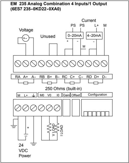
Voltage Unused Current PS PS L+ M 0-20mA 4-20mA M RA A+ A- RB B+ B- RC C+ C- RD D+ D- 250 Ohms (built-in) M L+ Gain Configuration 24 VDC Power
 EM 231 Analog Input, 8 Inputs
(6ES7 231-0HF22-0XA0)
Normal voltage input Short unused inputs A+ A- B+ B- C+ C- D+ D- E+ E- F+ F- S1 S2 M L+ G+ G- H+ H- Gain Configuration
0-20mA 4-20mA
- 24 VDC Power Supply PS PS L M Current inputs (switch 1 and 2 closed
 EM 232 Analog Output, 2 Outputs
(6ES7 232-0HB22-0XA0)
VLOAD ILOAD VLOAD ILOAD M0 V0 I0 M1 V1 I1 M L+ 24 VDC Power
 EM 232 Analog Output, 4 Outputs
(6ES7 232-0HD22-0XA0)
VLOAD ILOAD VLOAD ILOAD VLOAD ILOAD VLOAD ILOAD M0 V0 I0 M1 V1 I1 M2 V2 I2 M3 V3 I3 M L+
Figure A-13 Wiring Diagrams for Analog Expansion Modules
414
Technical Specifications Appendix A

Figure A-14 Wiring Diagrams for Analog Expansion Modules
Analog LED Indicators
The LED indicators for the analog modules are shown in Table A-19.
Table A-19 Analog LED Indicators
| LED Indicator | ON | OFF |
|---|---|---|
| 24 VDC Power Supply Good | No faults | No 24 VDC power |
Tip The state of user power is also reported in Special Memory (SM) bits. For more information, see Appendix D, SMB8 to SMB21 I/O Module ID and Error Registers.
415
S7-200 Programmable Controller System Manual
I nput Calibration
The calibration adjustments affect the instrumentation amplifier stage that follows the analog multiplexer (see the Input Block Diagram for the EM 231 in Figure A-17 and EM 235 in Figure A-19). Therefore, calibration affects all user input channels. Even after calibration, variations in the component values of each input circuit preceding the analog multiplexer will cause slight differences in the readings between channels connected to the same input signal.
To meet the specifications, you should enable analog input filters for all inputs of the module. Select 64 or more samples to calculate the average value.
To calibrate the input, use the following steps.
- Turn off the power to the module. Select the desired input range.
- Turn on the power to the CPU and module. Allow the module to stabilize for 15 minutes.
- Using a transmitter, a voltage source, or a current source, apply a zero value signal to one of the input terminals.
- Read the value reported to the CPU by the appropriate input channel.
- Adjust the OFFSET potentiometer until the reading is zero, or the desired digital data value.
- Connect a full-scale value signal to one of the input terminals. Read the value reported to the CPU.
- Adjust the GAIN potentiometer until the reading is 32000, or the desired digital data value.
- Repeat OFFSET and GAIN calibration as required.
C alibration and Configuration Location for EM 231 and EM 235
Figure A-15 shows the calibration potentiometer and configuration DIP switches located on the right of the bottom terminal block of the module.
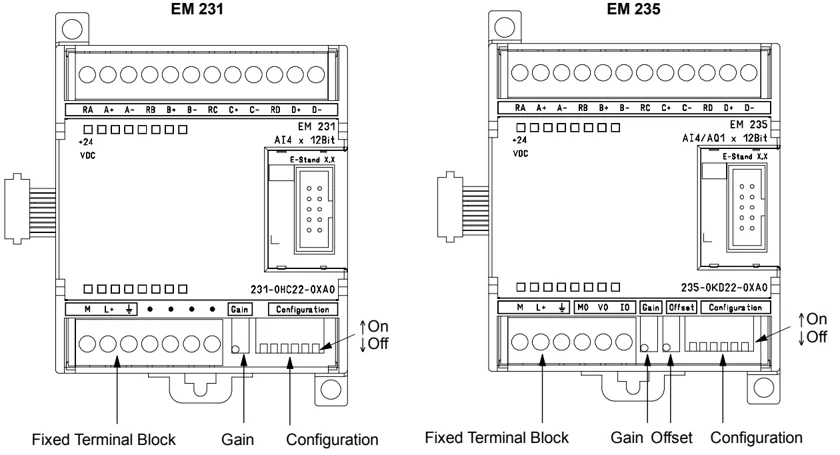
Figure A-15 Calibration Potentiometer and Configuration DIP Switch Location for the EM 231 and EM 235
416
Technical Specifications Appendix A
Configuration for EM 231
Table A-20 and Table A-21 show how to configure the the EM 231 modules using the configuration DIP switches. All inputs are set to the same analog input range. In these tables, ON is closed, and OFF is open. The switch settings are read only when the power is turned on.
For the EM 231 Analog Input, 4 Inputs module, switches 1, 2, and 3 select the analog input range (Table A-20).
Table A-20 Configuration Switch Table to Select Analog Input Range for the EM 231 Analog Input, 4 Inputs
For the EM 231 Analog Input, 8 Inputs module, switches 3, 4, and 5 select the analog input range. Use Switch 1 and 2 to select the current mode input (Table A-21). Switch 1 ON selects current mode input for Channel 6; OFF selects voltage mode. Switch 2 ON selects current mode input for Channel 7; OFF selects voltage mode.
Table A-21 EM 231 Configuration Switch Table to Select Analog Input Range for the EM 231 Analog Input, 8 Inputs
Configuration for EM 235 Table A-22 shows how to configure the EM 235 module using the configuration DIP switches. Switches 1 through 6 select the analog input range and resolution. All inputs are set to the same analog input range and format. Table A-22 shows how to select for unipolar/bipolar (switch 6), gain (switches 4 and 5), and attenuation (switches 1, 2, and 3). In these tables, ON is closed, and OFF is open. The switch settings are read only when the power is turned on.
Table A-22 EM 235 Configuration Switch Table to Select Analog Range and Resolution
418
Technical Specifications Appendix A
Input Data Word Format for EM 231 and EM 235
Figure A-16 shows where the 12-bit data value is placed within the analog input word of the CPU.
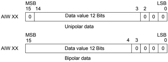
Figure A-16 Input Data Word Format for EM 231 and EM 235
Tip The 12 bits of the analog-to-digital converter (ADC) readings are left-justified in the data word format. The MSB is the sign bit: zero indicates a positive data word value. In the unipolar format, the three trailing zeros cause the data word to change by a count of eight for each one-count change in the ADC value. In the bipolar format, the four trailing zeros cause the data word to change by a count of sixteen for each one count change in the ADC value.
Input Block Diagrams for EM 231 and 235
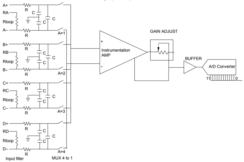
Figure A-17 Input Block Diagram for the EM 231 Analog Input, 4 Inputs
419
 Figure A-18 Input Block Diagram for the EM231 Analog Input, 8 Inputs
 Figure A-19 Input Block Diagram for the EM 235
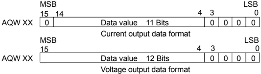
Output Data Word Format for EM 232 and EM 235
Figure A-20 shows where the 12-bit data value is placed within the analog output word of the CPU.
420
Technical Specifications Appendix A
MS B 15 14 4 3 LS B AQW XX 0 Data value 11 Bits 0 0 0 0 Current output data format
MS B 15 4 3 LS B AQW XX Data value 12 Bits 0 0 0 0 Voltage output data format
Figure A-20 Output Data Word Format for EM 232 and EM 235
Tip The 12 bits of the digital-to-analog converter (DAC) readings are left-justified in the output data word format. The MSB is the sign bit: zero indicates a positive data word value. The four trailing zeros are truncated before being loaded into the DAC registers. These bits have no effect on the output signal value.
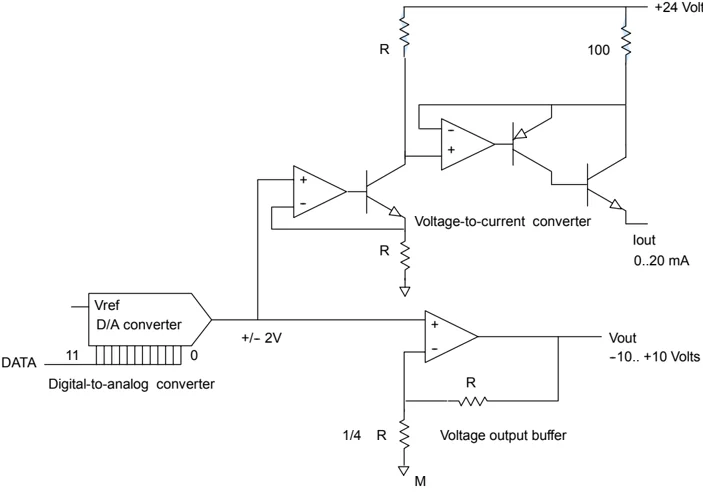
Output Block Diagram for EM 232 and EM 235

Figure A-21 Output Block Diagram for the EM 232 and EM 235
421
S7-200 Programmable Controller System Manual
I nstallation Guidelines
Use the following guidelines to ensure accuracy and repeatability:
☐ Ensure that the 24-VDC Sensor Supply is free of noise and is stable.
☐ Use the shortest possible sensor wires.
☐ Use shielded twisted pair wiring for sensor wires.
☐ Use a braided shield for best noise immunity.
☐ Terminate the shield at the Sensor location only.
☐ Short the inputs for any unused channels, as shown in Figure A-21.
☐ Avoid bending the wires into sharp angles.
☐ Use wireways for wire routing.
☐ Avoid placing signal wires parallel to high-energy wires. If the two wires must meet, cross them at right angles.
☐ Ensure that the input signals are within the common mode voltage specification by isolating the input signals or referencing them to the external 24V common of the analog module.
Tip The EM 231 and EM 235 expansion modules are not recommended for use with thermocouples.
Understanding the Analog Input Module: Accuracy and Repeatability
The EM 231 and EM 235 analog input modules are low-cost, high-speed 12 bit analog input modules. The modules can convert an analog signal input to its corresponding digital value in 149 µsec. The analog signal input is converted each time your program accesses the analog point. These conversion times must be added to the basic execution time of the instruction used to access the analog input.
The EM 231 and EM 235 provide an unprocessed digital value (no linearization or filtering) that corresponds to the analog voltage or current presented at the module's input terminals. Since the modules are high-speed modules, they can follow rapid changes in the analog input signal (including internal and external noise).
You can minimize reading-to-reading variations caused by noise for a constant or slowly changing analog input signal by averaging a number of readings. Note that increasing the number of readings used in computing the average value results in a correspondingly slower response time to changes in the input signal.
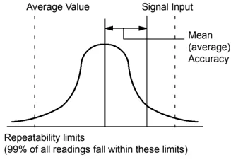
Figure A-22 shows the 99% repeatability limits, the mean or average value of the individual readings, and the mean accuracy in a graphical form.
The specifications for repeatability describe the reading-to-reading variations of the module for an input signal that is not changing. The repeatability specification defines the limits within which 99% of the readings will fall. The repeatability is described in this figure by the bell curve.
The mean accuracy specification describes the average value of the error (the difference between the average value of individual readings and the exact value of the actual analog input signal).
Table A-23 gives the repeatability specifications and the mean accuracy as they relate to each of the configurable ranges.
422
Definitions of the Analog Specifications
Accuracy: deviation from the expected value on a given point
Resolution: the effect of an LSB change reflected on the output.
Table A-23 EM 231 and EM 235 S specifications
1 Measurements made after the selected input range has been calibrated.
2 The offset error in the signal near zero analog input is not corrected, and is not included in the accuracy specifications.
3 There is a channel-to-channel carryover conversion error, due to the finite settling time of the analog multiplexer. The maximum carryover error is 0.1% of the difference between channels.
4 Mean accuracy includes effects of non-linearity and drift from 0 to 55 degrees C.
5 Analog input accuracy may deviate up to +/-10% of full scale when subjected to severe RF interferences such as specified in the product standard EN 61131-2:2007. Following the recommended installation guidelines on the previous page can minimize unintended disturbances on analog inputs. For high frequency immunity it is recommended that the cable shield be terminated at both ends.
Thermocouple and RTD Expansion Modules Specifications
Table A-24 Thermocouple and RTD Modules Order Numbers
| Order Number | Expansion Model | EM Inputs | EM Outputs | Removable Connector |
|---|---|---|---|---|
| 6ES7 231-7PD22-0XA0 | EM 231 Analog Input Thermocouple, 4 Inputs | 4 Thermocouple | - | No |
| 6ES7 231-7PF22-0XA0 | EM 231 Analog Input Thermocouple, 8 Inputs | 8 Thermocouple | - | No |
| 6ES7 231-7PB22-0XA0 | EM 231 Analog Input RTD, 2 Inputs | 2 RTD | - | No |
| 6ES7 231-7PC22-0XA0 | EM 231 Analog Input RTD, 4 Inputs | 4 RTD | - | No |
Table A-25 Thermocouple and RTD Modules General Specifications
| Order Number | Module Name and Description | Dimensions (mm) (W x H x D) | Weight | Dissipation | VDC Requirements +5 VDC | +24 VDC |
|---|---|---|---|---|---|---|
| 6ES7 231-7PD22-0XA0 | EM 231 Analog Input Thermocouple, 4 Inputs | 71.2 x 80 x 62 | 210 g | 1.8 W | 87 mA | 60 mA |
| 6ES7 231-7PF22-0XA0 | EM 231 Analog Input Thermocouple, 8 Inputs | 71.2 x 80 x 62 | 210 g | 1.8 W | 87 mA | 60 mA |
| 6ES7 231-7PB22-0XA0 | EM 231 Analog Input RTD, 2 Inputs | 71.2 x 80 x 62 | 210 g | 1.8 W | 87 mA | 60 mA |
| 6ES7 231-7PC22-0XA0 | EM 231 Analog Input RTD, 4 Inputs | 71.2 x 80 x 62 | 210 g | 1.8 W | 87 mA | 60 mA |
Table A-26 Thermocouple and RTD Modules Specifications
| General | 6ES7 231-7PD22-0XA0 Thermocouple, 4 Inputs | 6ES7 231-7PF22-0XA0 Thermocouple, 8 Inputs | 6ES7 231-7PB22-0XA0 RTD, 2 Inputs | 6ES7 231-7PC22-0XA0 RTD, 4 Inputs |
|---|---|---|---|---|
| Isolation | ||||
| Field to logic | 500 VAC | 500 VAC | ||
| Field to 24 VDC | 500 VAC | 500 VAC | ||
| 24 VDC to logic | 500 VAC | 500 VAC | ||
| Common mode input range (input channel to input channel) | 120 VAC | 0 | ||
| Common mode rejection | > 120 dB at 120 VAC | > 120 dB at 120 VAC | ||
| Input type | Floating TC | Module ground referenced RTD (2, 3, or 4 wire connections) | ||
| Input ranges¹ | TC types (select one per module) S, T, R, E, N, K, J Voltage range : +/- 80 mV | RTD types (select one per module): platinum (Pt), copper (Cu), nickel (Ni), or Resistance See Table A-31 or A-32 for available RTD types. | ||
| Input resolution | ||||
| Temperature | 0.1° C / 0.1° F | 0.1° C / 0.1° F | ||
| Voltage | 15 bits plus sign | - | ||
| Resistance | - | 15 bits plus sign resistive | ||
| Measuring Principle | Sigma-delta | Sigma-delta | ||
| Module update time: All channels | 405 ms | 810 ms | 405 ms (700 ms for Pt10000) | 810 ms (1400 ms for Pt10000) |
| Wire length | 100 meters to sensor max. | 100 meters to sensor max. | ||
| Wire loop resistance | 100Ω max. | 20Ω, 2.7Ω for Cu max. | 20Ω, 2.7Ω for 10Ω RTDs | |
| Suppression of interference | 85 dB at 50 Hz/60 Hz/400 Hz | 85 dB at 50 Hz/60 Hz/400 Hz | ||
| Data word format | Voltage: -27648 to + 27648 | Resistance: 0 to +27648 | ||
| Maximum sensor dissipation | - | 1m W | ||
| Input impedance | ≥1 MΩ | ≥ 10 MΩ | ||
| Maximum input voltage | 30 VDC | 30 VDC (sense), 5 VDC (source) | 30 VDC | |
| Input filter attenuation | -3 db at 21 kHz | -3 db at 3.6 kHz | -3 db at 21 kHz | |
| Basic error | 0.1% FS (voltage) | 0.1% FS (resistance) | ||
| Repeatability | 0.05% FS | 0.05% FS | ||
| Cold junction error | ±1.5 ° C | - | ||
| LED indicator | 2 (External 24 VDC present and System Fail) | |||
| 24 VDC supply voltage range | 20.4 to 28.8 VDC (Class 2, Limited Power, or sensor power from PLC) |
¹ The input range selection (temperature, voltage on resistance) applies to all channels on the module.
424
Technical Specifications Appendix A
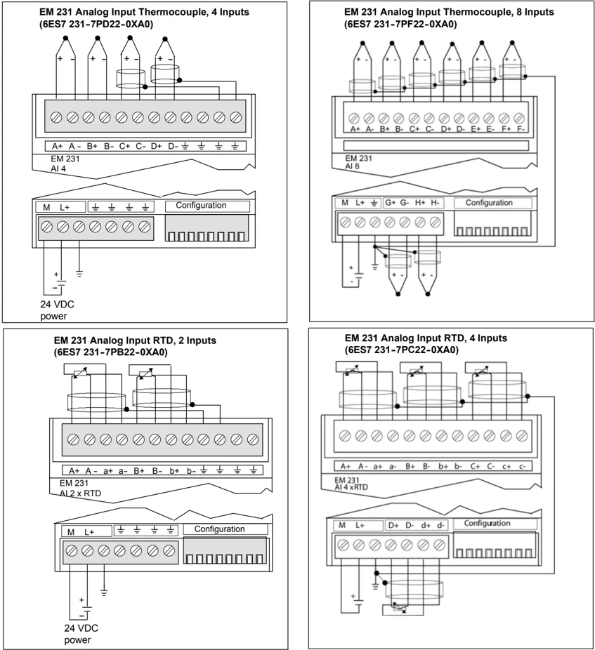
Figure A-23 Connector Terminal Identification for EM 231 Thermocouple and EM 231 RTD Modules
Compatibility
The RTD and Thermocouple modules are designed to work with the CPU 222, CPU 224, CPU 224XP and CPU 226.
Tip The RTD and Thermocouple modules are designed to give maximum performance when installed in a stable temperature environment.
The EM 231 Thermocouple module, for example, has special cold junction compensation circuitry that measures the temperature at the module connectors and makes necessary changes to the measurement to compensate for temperature differences between the reference temperature and the temperature at the module. If the ambient temperature is changing rapidly in the area where the EM 231 Thermocouple module is installed, additional errors are introduced.
To achieve maximum accuracy and repeatability, Siemens recommends that the S7-200 RTD and Thermocouple modules be mounted in locations that have stable ambient temperature.
Noise Immunity
Use shielded wires for best noise immunity. If a thermocouple input channel is not used, short the unused channel inputs, or connect them in parallel to another channel.
EM 231 Thermocouple Module
The EM 231 Thermocouple module provides a convenient, isolated interface for the S7-200 family to seven thermocouple types: J, K, E, N, S, T, and R. It allows the S7-200 to connect to low level analog signals, ±80mV range. All thermocouples attached to the module must be of the same type.
Thermocouple Basics
Thermocouples are formed whenever two dissimilar metals are electrically bonded to each other. A voltage is generated that is proportional to the junction temperature. This voltage is small; one microvolt could represent many degrees. Measuring the voltage from a thermocouple, compensating for extra junctions, and then linearizing the result forms the basis of temperature measurement using thermocouples.
When you connect a thermocouple to the EM 231 Thermocouple Module, the two dissimilar metal wires are attached to the module at the module signal connector. The place where the two dissimilar wires are attached to each other forms the sensor thermocouple.
Two more thermocouples are formed where the two dissimilar wires are attached to the signal connector. The connector temperature causes a voltage that adds to the voltage from the sensor thermocouple. If this voltage is not corrected, then the temperature reported will deviate from the sensor temperature.
Cold junction compensation is used to compensate for the connector thermocouple. Thermocouple tables are based on a reference junction temperature, usually zero degrees Celsius. The cold junction compensation compensates the connector to zero degrees Celsius. The cold junction compensation restores the voltage added by the connector thermocouples. The temperature of the module is measured internally, then converted to a value to be added to the sensor conversion. The corrected sensor conversion is then linearized using the thermocouple tables.
Configuring the EM 231 Thermocouple Module
Configuration DIP switches located on the bottom of the module allow you to select the thermocouple type, open wire detect, temperature scale, and cold junction compensation. For the DIP switch settings to take effect, you need to power cycle the PLC and/or the user 24V power supply.
DIP switch 4 is reserved for future use. Set DIP switch 4 to the 0 (down or off) position. Table A-27 shows other DIP switch settings.
426
Technical Specifications Appendix A
Table A-27 Configuring the Thermocouple Module DIP Switches
| Switches 1,2,3 | Thermocouple Type | Setting | Description |
|---|---|---|---|
| SW1, 2, 3Configuration↑1 - On↓0 - Off*Set DIP switch 4to the 0 (down) position. | J (Default) | 000 | Switches 1 to 3 select the thermocouple type(or mV operation) for all channels on themodule. For example, for an E type,thermocouple SW1 = 0, SW2 = 1, SW3 = 1. |
| K | 001 | ||
| T | 010 | ||
| E | 011 | ||
| R | 100 | ||
| S | 101 | ||
| N | 110 | ||
| +/-80mV | 111 |
| Switch 5 | Open Wire Detect Direction | Setting | Description |
|---|---|---|---|
| SW5Configuration↑1 - On↓0 - Off | Upscale(+3276.7 degrees) | 0 | 0 indicates positive on open wire1 indicates negative on open wire |
| Downscale(-3276.8 degrees) | 1 |
| Switch 6 | Open Wire Detect Enable | Setting | Description |
|---|---|---|---|
| SW6Configuration↑1 - On↓0 - Off | Enable | 0 | Open wire detection is performed by injectinga 25 μA current onto the input terminals. Theopen wire enable switch enables or disablesthe current source. The open wire rangecheck is always performed, even when thecurrent source is disabled. The EM 231Thermocouple module detects open wire if theinput signal exceeds approximately ±200mV.When an open wire is detected, the modulereading is set to the value selected by theOpen Wire Detect. |
| Disable | 1 |
| Switch 7 | Temperature Scale | Setting | Description |
|---|---|---|---|
| SW7Configuration↑1 - On↓0 - Off | Celsius (°C) | 0 | The EM 231 Thermocouple module can reporttemperatures in Celsius or Fahrenheit. TheCelsius to Fahrenheit conversion is performedinside the module. |
| Fahrenheit (°F) | 1 |
| Switch 8 | Cold Junction | Setting | Description |
|---|---|---|---|
| SW8Configuration↑1 - On↓0 - Off | Cold junctioncompensation enabled | 0 | Cold junction compensation must be enabledwhen you are using thermocouples. If coldjunction compensation is not enabled, theconversions from the module will be in errorbecause of the voltage that is created whenthe thermocouple wire is connected to themodule connector. Cold junction isautomatically disabled when you select the±80mV range. |
| Cold junctioncompensation disabled | 1 |
427
Tip
- The open wire current source could interfere with signals from some low level sources such as thermocouple simulators.
- Input voltages exceeding approximately ±200mV will trigger open wire detection even when the open wire current source is disabled.
Tip
- Module error could exceed specifications while the ambient temperature is changing.
- Exceeding the module ambient temperature range specification could cause the module cold junction to be in error.
Using the Thermocouple: Status Indicators
The EM 231 Thermocouple module provides the PLC with data words that indicate temperatures or error conditions. Status bits indicate range error and user supply/module failure. LEDs indicate the status of the module. Your program should have logic to detect error conditions and respond appropriately for the application. Table A-28 shows the EM 231 Thermocouple status indicators.
Table A-28 EM 231 Thermocouple Status Indicators
| Error Condition | Channel Data | SF LED Red | 24 V LED Green | Range Status Bit¹ | 24 VDC User Power Bad² |
|---|---|---|---|---|---|
| No errors | Conversion data | OFF | ON | 0 | 0 |
| 24 V missing | 32766 | OFF | OFF | 0 | 1 |
| Open wire and current source enabled | -32768/32767 | BLINK | ON | 1 | 0 |
| Out of range input | -32768/32767 | BLINK | ON | 1 | 0 |
| Diagnostic error³ | 0000 | ON | OFF | 0 | note ³ |
¹ Range status bit is bit 3 in module error register byte (SMB9 for Module 1, SMB11 for Module 2, etc.)
² User Power Bad status bit is bit 2 in module error register byte (SMB 9, SMB 11, etc., refer to Appendix D)
³ Diagnostic errors cause a module configuration error. The User Power Bad status bit may or may not be set before the module configuration error.
Tip
The channel data format is two’s complement, 16-bit words. Temperature is presented in 0.1 degree units. For example, if the measured temperature is 100.2 degrees, the reported data is 1002. Voltage data are scaled to 27648. For example, -60.0mV is reported as -20736 (=-60mV/80mV *27648).
If the PLC has read the data:
- All 4 channels in the EM 231 Analog Input Thermocouple 4 Inputs are updated every 405 milliseconds.
- All channels in the EM 231 Analog Input Thermocouple 8 Inputs are updated every 810 milliseconds.
If the PLC does not read the data within one update time, the module reports old data until the next module update after the PLC read. To keep channel data current, it is recommended that the PLC program read data at least as often as the module update rate.
Tip
When you are using the EM 231 Thermocouple module, you should disable analog filtering in the PLC. Analog filtering can prevent error conditions from being detected in a timely manner.
428
Technical Specifications Appendix A
Table A-29 Temperature Ranges (°C) and Accuracy for Thermocouple Types
| Data Word (1 digit = 0.1°C) | Type J | Type K | Type T | Type E | Type R, S | Type N | ±80mV | ||
|---|---|---|---|---|---|---|---|---|---|
| Dec | Hex | ||||||||
| 32767 | 7FFF | >1200.0 °C | >1372.0 °C | >400.0 °C | >1000.0°C | >1768.0°C | >1300.0°C | >94.071mV | OF |
| ↑ | ↑ | ↑ | ↑ | ||||||
| 32511 | 7EFF | 94.071mV | OR | ||||||
| : | : | 80.0029mV | |||||||
| 27649 | 6C01 | 80mV | |||||||
| 27648 | 6C00 | ↑ | |||||||
| : | : | ||||||||
| 17680 | 4510 | ↑ | 1768.0°C | ||||||
| : | : | ↑ | |||||||
| 13720 | 3598 | 1372.0°C overrange | 1300.0°C | NR | |||||
| : | : | ||||||||
| 13000 | 32C8 | ↑ | 1300.0°C | ||||||
| : | : | ||||||||
| 12000 | 2EE0 | 1200.0°C | ↑ | ||||||
| : | : | ||||||||
| 10000 | 2710 | 1000.0°C | |||||||
| : | : | ||||||||
| 4000 | 0FA0 | 400.0°C | 400.0°C | ||||||
| : | : | ||||||||
| 1 | 0001 | 0.1°C | 0.1°C | 0.1°C | 0.1°C | 0.1°C | 0.1°C | 0.0029mV | |
| 0 | 0000 | 0.0°C | 0.0°C | 0.0°C | 0.0°C | 0.0°C | 0.0°C | 0.0mV | |
| -1 | FFFF | -0.1°C | -0.1°C | -0.1°C | -0.1°C | -0.1°C | -0.1°C | -0.0029mV | |
| : | : | underrange | |||||||
| -500 | FE0C | -50.0°C | |||||||
| -1500 | FA24 | -150.0°C | |||||||
| : | : | ||||||||
| -2000 | F830 | underrange | -200.0°C | ||||||
| : | : | ||||||||
| -2100 | F7CC | -210.0°C | |||||||
| : | : | ||||||||
| -2400 | F6A0 | -240.0°C | |||||||
| : | : | underrange | underrange | ||||||
| -2550 | F60A | -255.0°C | |||||||
| : | : | underrange | |||||||
| -2700 | F574 | ↓ | -270.0°C | -270.0°C | -270.0°C | -270.0°C | NR | ||
| : | : | ||||||||
| -27648 | 9400 | ↓ | ↓ | ↓ | ↓ | -80.mV | |||
| -27649 | 93FF | -80.0029mV | |||||||
| : | : | ||||||||
| -32512 | 8100 | -94.071mV | UR | ||||||
| ↓ | ↓ | ↓ | ↓ | ||||||
| -32768 | 8000 | <-210.0°C | <-270.0°C | <-270.0°C | <-270.0°C | <-50.0°C | <-270.0°C | <-94.071mV | UF |
| Accuracy over full span | ±0.1% | ±0.3% | ±0.6% | ±0.3% | ±0.6% | ±0.4% | ±0.1% | ||
| Accuracy (normal range without cold junction) | ±1.5°C | ±1.7°C | ±1.4°C | ±1.3°C | ±3.7°C | ±1.6°C | ±0.10% | ||
| Cold junction error | ±1.5°C | ±1.5°C | ±1.5°C | ±1.5°C | ±1.5°C | ±1.5°C | N/A | ||
| *OF = Overflow; OR = Overrange; NR = Normal range; UR = Underrange; UF = Underflow | |||||||||
| ↑ indicates that all analog values greater than this and below the open wire threshold report the overflow data value, 32767 (0x7FFF). | |||||||||
| ↓ indicates that all analog values less than this and greater than the open wire threshold report the underflow data value, -32768 (0x8000). |
429
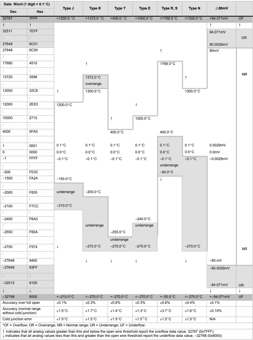
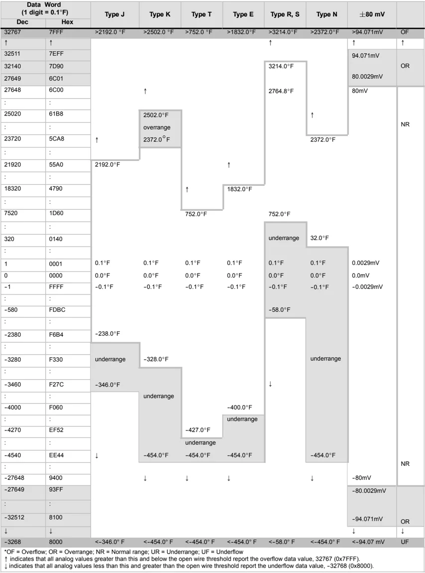
Table A-30 Temperature Ranges (°F) for Thermocouple Types
| Data Word (1 digit = 0.1°F) | Type J | Type K | Type T | Type E | Type R, S | Type N | ±80 mV | |
|---|---|---|---|---|---|---|---|---|
| Dec | Hex | |||||||
| 32767 | 7FFF | >2192.0 °F | >2502.0 °F | >752.0 °F | >1832.0°F | >3214.0°F | >2372.0°F | >94.071mV |
| ↑ | ↑ | OF | ||||||
| 32511 | 7EFF | |||||||
| 32140 | 7D90 | 3214.0°F | 94.071mV | |||||
| 27649 | 6C01 | 2764.8°F | 80.0029mV | |||||
| 27648 | 6C00 | ↑ | ↑ | 80mV | ||||
| : | : | |||||||
| 25020 | 61B8 | 2502.0°F | ||||||
| : | : | overrange | ||||||
| 23720 | 5CA8 | ↑ | 2372.0°F | 2372.0°F | OR | |||
| : | : | |||||||
| 21920 | 55A0 | 2192.0°F | ↑ | NR | ||||
| : | : | |||||||
| 18320 | 4790 | 1832.0°F | ||||||
| : | : | ↑ | ||||||
| 7520 | 1D60 | 752.0°F | 752.0°F | |||||
| : | : | |||||||
| 320 | 0140 | underrange | 32.0°F | |||||
| : | : | |||||||
| 1 | 0001 | 0.1°F | 0.1°F | 0.1°F | 0.1°F | 0.1°F | 0.1°F | 0.0029mV |
| 0 | 0000 | 0.0°F | 0.0°F | 0.0°F | 0.0°F | 0.0°F | 0.0°F | 0.0mV |
| -1 | FFFF | -0.1°F | -0.1°F | -0.1°F | -0.1°F | -0.1°F | -0.1°F | -0.0029mV |
| : | : | |||||||
| -580 | FDBC | -58.0°F | ||||||
| : | : | |||||||
| -2380 | F6B4 | -238.0°F | ||||||
| : | : | |||||||
| -3280 | F330 | underrange | -328.0°F | underrange | ||||
| : | : | |||||||
| -3460 | F27C | -346.0°F | ||||||
| : | : | underrange | ↓ | |||||
| -4000 | F060 | -400.0°F | ||||||
| : | : | underrange | ||||||
| -4270 | EF52 | -427.0°F | ||||||
| : | : | underrange | ||||||
| -4540 | EE44 | ↓ | -454.0°F | -454.0°F | -454.0°F | -454.0°F | NR | |
| : | : | |||||||
| -27648 | 9400 | ↓ | ↓ | ↓ | ↓ | -80mV | ||
| -27649 | 93FF | -80.0029mV | ||||||
| : | : | |||||||
| -32512 | 8100 | -94.071mV | OR | |||||
| ↓ | ↓ | ↓ | ↓ | |||||
| -3268 | 8000 | <-346.0°F | <-454.0°F | <-454.0°F | <-454.0°F | <-58.0°F | <-454.0°F | <-94.07 mV |
| UF |
*OF = Overflow; OR = Overrange; NR = Normal range; UR = Underrange; UF = Underflow ↑ indicates that all analog values greater than this and below the open wire threshold report the overflow data value, 32767 (0x7FFF). ↓ indicates that all analog values less than this and greater than the open wire threshold report the underflow data value, -32768 (0x8000).
430
EM 231 RTD Module
The EM 231 RTD module provides a convenient interface for the S7-200 family to several different RTDs. It also allows the S7-200 to measure three different resistance ranges. All RTDs attached to the module must be of the same type.
Configuring the EM 231 RTD Module
DIP switches enable you to select RTD type, wiring configuration, temperature scale, and burnout direction. The DIP switches are located on the bottom of the module as shown in Figure A-24. For the DIP switch settings to take effect, you need to power cycle the PLC and/or the user 24V power supply.
Select RTD type by setting DIP switches 1, 2, 3, 4, 5 and 6 to correspond to the RTD as shown in Table A-31 and Table A-32. Refer to Table A-33 for other DIP switch settings.
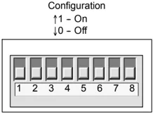
Figure A-24 DIP Switches for the EM 231 RTD Module
Table A-31 Selecting the RTD Type: DIP Switches 1 to 6 for the EM 231 Analog Input RTD 4 Inputs
| RTD Type and Alpha¹ | SW1 | SW2 | SW3 | SW4 | SW5 | SW6 | RTD Type and Alpha¹ | SW1 | SW2 | SW3 | SW4 | SW5 | SW6 |
|---|---|---|---|---|---|---|---|---|---|---|---|---|---|
| 100Ω Pt 0.003850 (Default) | 0 | 0 | 0 | 0 | 0 | 0 | 100Ω Pt 0.003902 | 1 | 0 | 0 | 0 | 0 | 0 |
| 200Ω Pt 0.003850 | 0 | 0 | 0 | 0 | 1 | 0 | 200Ω Pt 0.003902 | 1 | 0 | 0 | 0 | 1 | 0 |
| 500Ω Pt 0.003850 | 0 | 0 | 0 | 1 | 0 | 0 | 500Ω Pt 0.003902 | 1 | 0 | 0 | 1 | 0 | 0 |
| 1000Ω Pt 0.003850 | 0 | 0 | 0 | 1 | 1 | 0 | 1000Ω Pt 0.003902 | 1 | 0 | 0 | 1 | 1 | 0 |
| 100Ω Pt 0.003920 | 0 | 0 | 1 | 0 | 0 | 0 | SPARE | 1 | 0 | 1 | 0 | 0 | 0 |
| 200Ω Pt 0.003920 | 0 | 0 | 1 | 0 | 1 | 0 | 100Ω Ni 0.00672 | 1 | 0 | 1 | 0 | 1 | 0 |
| 500Ω Pt 0.003920 | 0 | 0 | 1 | 1 | 0 | 0 | 120Ω Ni 0.00672 | 1 | 0 | 1 | 1 | 0 | 0 |
| 1000Ω Pt 0.003920 | 0 | 0 | 1 | 1 | 1 | 0 | 1000Ω Ni 0.00672 | 1 | 0 | 1 | 1 | 1 | 0 |
| 100Ω Pt 0.00385055 | 0 | 1 | 0 | 0 | 0 | 0 | 100Ω Ni 0.006178 | 1 | 1 | 0 | 0 | 0 | 0 |
| 200Ω Pt 0.00385055 | 0 | 1 | 0 | 0 | 1 | 0 | 120Ω Ni 0.006178 | 1 | 1 | 0 | 0 | 1 | 0 |
| 500Ω Pt 0.00385055 | 0 | 1 | 0 | 1 | 0 | 0 | 1000Ω Ni 0.006178 | 1 | 1 | 0 | 1 | 0 | 0 |
| 1000Ω Pt 0.00385055 | 0 | 1 | 0 | 1 | 1 | 0 | 10000Ω Pt 0.003850 | 1 | 1 | 0 | 1 | 1 | 0 |
| 100Ω Pt 0.003916 | 0 | 1 | 1 | 0 | 0 | 0 | 10Ω Cu 0.004270 | 1 | 1 | 1 | 0 | 0 | 0 |
| 200Ω Pt 0.003916 | 0 | 1 | 1 | 0 | 1 | 0 | 150Ω FS Resistance | 1 | 1 | 1 | 0 | 1 | 0 |
| 500Ω Pt 0.003916 | 0 | 1 | 1 | 1 | 0 | 0 | 300Ω FS Resistance | 1 | 1 | 1 | 1 | 0 | 0 |
| 1000Ω Pt 0.003916 | 0 | 1 | 1 | 1 | 1 | 0 | 600Ω FS Resistance | 1 | 1 | 1 | 1 | 1 | 0 |
| GOST 50Ω Pt 0.00385055 | 0 | 0 | 0 | 0 | 1 | 1 | GOST Cu 50Ω 0.00426 | 0 | 1 | 0 | 1 | 1 | 1 |
| GOST 100Ω Pt 0.00385055 | 0 | 0 | 0 | 1 | 0 | 1 | GOST Cu 100Ω 0.00426 | 0 | 1 | 1 | 0 | 0 | 1 |
| GOST 500Ω Pt 0.00385055 | 0 | 0 | 0 | 1 | 1 | 1 | GOST Cu 500Ω 0.00426 | 0 | 1 | 1 | 0 | 1 | 1 |
| GOST 10Ω Pt 0.003910 | 0 | 0 | 1 | 0 | 0 | 1 | GOST Cu 10Ω 0.00428 | 0 | 1 | 1 | 1 | 0 | 1 |
| GOST 500Ω Pt 0.003910 | 0 | 0 | 1 | 0 | 1 | 1 | GOST Cu 50Ω 0.00428 | 0 | 1 | 1 | 1 | 1 | 1 |
| GOST 100Ω Pt 0.003910 | 0 | 0 | 1 | 1 | 0 | 1 | GOST Cu 100Ω 0.00428 | 1 | 0 | 0 | 0 | 0 | 1 |
| GOST 500Ω Pt 0.003910 | 0 | 0 | 1 | 1 | 1 | 1 | GOST Cu 500Ω 0.00428 | 1 | 0 | 0 | 0 | 1 | 1 |
Table A-31 Selecting the RTD Type: DIP Switches 1 to 6 for the EM 231 Analog Input RTD 4 Inputs
| RTD Type and Alpha¹ | SW1 | SW2 | SW3 | SW4 | SW5 | SW6 | RTD Type and Alpha¹ | SW1 | SW2 | SW3 | SW4 | SW5 | SW6 |
|---|---|---|---|---|---|---|---|---|---|---|---|---|---|
| GOST 10Ω Pt 0.003910 | 0 | 1 | 0 | 0 | 0 | 1 | Spare | 1 | 0 | 0 | 1 | 0 | 1 |
| LG-Ni 1000Ω Pt 0.005000 | 0 | 1 | 0 | 0 | 1 | 1 |
¹ All RTDs represent 0° C. at the listed resistance except for Cu 10 ohm. Cu 10 ohm is 25° C. at 10 ohm and 0° C. at 9.035 ohm.
Table A-32 Selecting the RTD Type: DIP Switches 1 to 5 for the EM 231 Analog Input RTD 2 Inputs
| RTD Type and Alpha¹ | SW1 | SW2 | SW3 | SW4 | SW5 | RTD Type and Alpha¹ | SW1 | SW2 | SW3 | SW4 | SW5 |
|---|---|---|---|---|---|---|---|---|---|---|---|
| 100Ω Pt 0.003850 (Default) | 0 | 0 | 0 | 0 | 0 | 100Ω Pt 0.003902 | 1 | 0 | 0 | 0 | 0 |
| 200Ω Pt 0.003850 | 0 | 0 | 0 | 0 | 1 | 200Ω Pt 0.003902 | 1 | 0 | 0 | 0 | 1 |
| 500Ω Pt 0.003850 | 0 | 0 | 0 | 1 | 0 | 500Ω Pt 0.003902 | 1 | 0 | 0 | 1 | 0 |
| 1000Ω Pt 0.003850 | 0 | 0 | 0 | 1 | 1 | 1000Ω Pt 0.003902 | 1 | 0 | 0 | 1 | 1 |
| 100Ω Pt 0.003920 | 0 | 0 | 1 | 0 | 0 | SPARE | 1 | 0 | 1 | 0 | 0 |
| 200Ω Pt 0.003920 | 0 | 0 | 1 | 0 | 1 | 100Ω Ni 0.00672 | 1 | 0 | 1 | 0 | 1 |
| 500Ω Pt 0.003920 | 0 | 0 | 1 | 1 | 0 | 120Ω Ni 0.00672 | 1 | 0 | 1 | 1 | 0 |
| 1000Ω Pt 0.003920 | 0 | 0 | 1 | 1 | 1 | 1000Ω Ni 0.00672 | 1 | 0 | 1 | 1 | 1 |
| 100Ω Pt 0.00385055 | 0 | 1 | 0 | 0 | 0 | 100Ω Ni 0.006178 | 1 | 1 | 0 | 0 | 0 |
| 200Ω Pt 0.00385055 | 0 | 1 | 0 | 0 | 1 | 120Ω Ni 0.006178 | 1 | 1 | 0 | 0 | 1 |
| 500Ω Pt 0.00385055 | 0 | 1 | 0 | 1 | 0 | 1000Ω Ni 0.006178 | 1 | 1 | 0 | 1 | 0 |
| 1000Ω Pt 0.00385055 | 0 | 1 | 0 | 1 | 1 | 10000Ω Pt 0.003850 | 1 | 1 | 0 | 1 | 1 |
| 100Ω Pt 0.003916 | 0 | 1 | 1 | 0 | 0 | 10Ω Cu 0.004270 | 1 | 1 | 1 | 0 | 0 |
| 200Ω Pt 0.003916 | 0 | 1 | 1 | 0 | 1 | 150Ω FS Resistance | 1 | 1 | 1 | 0 | 1 |
| 500Ω Pt 0.003916 | 0 | 1 | 1 | 1 | 0 | 300Ω FS Resistance | 1 | 1 | 1 | 1 | 0 |
| 1000Ω Pt 0.003916 | 0 | 1 | 1 | 1 | 1 | 600Ω FS Resistance | 1 | 1 | 1 | 1 | 1 |
¹ All RTDs represent 0° C. at the listed resistance except for Cu 10 ohm. Cu 10 ohm is 25° C. at 10 ohm and 0° C. at 9.035 ohm.
432
Technical Specifications Appendix A
Table A-33 Setting RTD DIP Switches for the EM 231 Analog Input RTD Module
\begin{tabular}{|p{0.25\textwidth}|p{0.2\textwidth}|c|p{0.3\textwidth}|} \hline \textbf{Switch 6 (2 Channel Module Only)} & \textbf{Open Wire Detect/ Out of Range} & \textbf{Setting} & \textbf{Description} \ \hline SW6 \newline Configuration \newline \uparrow1 - On \newline \downarrow0 - Off \newline 1 2 3 4 5 6 7 8 & Upscale (+3276.7 degrees) & 0 & Indicates positive on open wire or out of range \ \cline{2-4} & Downscale (-3276.8 degrees) & 1 & Indicates negative on open wire or out of range \ \hline \textbf{Switch 7 (Both Modules)} & \textbf{Temperature Scale} & \textbf{Setting} & \textbf{Description} \ \hline SW7 \newline Configuration \newline \uparrow1 - On \newline \downarrow0 - Off \newline 1 2 3 4 5 6 7 8 & Celsius (°C) & 0 & The RTD module can report temperatures in Celsius or Fahrenheit. The Celsius to Fahrenheit conversion is performed inside the module. \ \cline{2-4} & Fahrenheit (°F) & 1 & \ \hline \textbf{Switch 8 (Both Modules)} & \textbf{Wiring Scheme} & \textbf{Setting} & \textbf{Description} \ \hline SW8 \newline Configuration \newline \uparrow1 - On \newline \downarrow0 - Off \newline 1 2 3 4 5 6 7 8 & 3-wire & 0 & You can wire the RTD module to the sensor in three ways (shown in the figure). The most accurate is 4 wire). The least accurate is 2 wire, which is only recommended if errors due to wiring can be ignored in your application. \ \cline{2-4} & 2-wire or 4-wire & 1 & \ \hline \end{tabular}
 RTD 4 Wire
(most accurate)
A+ Sense + A- Sense - a+ Source + a- Source -
$R_{L1}$ $R_{L2}$ RTD
RTD 3 Wire
A+ Sense + A- Sense - a+ Source + a- Source -
$R_{L1}$ $R_{L2}$ RTD
If $R_{L1}=R_{L2}$, error is minimal.
RTD 2 Wire
Set switch to 4-wire mode.
A+ Sense + A- Sense - a+ Source + a- Source -
$R_{L1}$ $R_{L2}$ RTD
R_L1+R_L2=Error
Note: $R_{L1}$ = Lead resistance from a+ terminal to the RTD $R_{L2}$ = Lead resistance from a- terminal to the RTD
Figure A-25 Wiring the RTD to the Sensor by 4, 3, and 2 Wire
433
S7-200 Programmable Controller System Manual
EM 231 RTD Status Indicators
The RTD module provides the PLC with data words that indicate temperatures or error conditions. Status bits indicate range error and user supply/module failure. LEDs indicate the status of the module. Your program should have logic to detect error conditions and respond appropriately for the application. Table A-34 shows the status indicators provided by the EM 231 RTD module.
Tip The channel data format is twos complement, 16-bit words. Temperature is presented in 0.1 degree units. (For example, if the measured temperature is 100.2 degrees, the reported data is 1002.) Resistance data are scaled to 27648. For example, 75% of full scale resistance is reported as 20736. (225\Omega /300\Omega *27648 = 20736)
Table A-34 EM 231 RTD Status Indicators
1 Range status bit is bit 3 in module error register byte (SMB9 for Module 1, SMB11 for Module 2, etc.) 2 User Power Bad status bit is bit 2 in module error register byte (such as SMB 9, SMB 11, refer to Appendix D.) 3 Diagnostic errors cause a module configuration error. The User Power Bad status bit may or may not be set before the module configuration error.
If the PLC has read the data:
☐ All 4 channels in the EM 231 Analog Input RTD 2 Inputs are updated every 405 milliseconds.
☐ All channels in the EM 231 Analog Input RTD 4 Inputs are updated every 810 milliseconds.
If the PLC does not read the data within one update time, the module reports old data until the next module update after the PLC read. To keep channel data current, it is recommended that the PLC program read data at least as often as the module update rate.
Tip When you are using the RTD module, be sure to disable analog filtering in the PLC. Analog filtering can prevent error conditions from being detected in a timely manner.
Open wire detection is performed by software internal to the RTD module. Out of range inputs and detected open wire conditions are signaled by setting the range status bit in the SMB and by setting the channel data up or down scale per the switch settings. Open wire detection takes a minimum of three module scan cycles and can take longer, depending on which wire(s) are open. Open Source+ and/or Source- wires are detected in the minimum time. Open Sense+ and/or Sense- wires can take 5 seconds or more to detect. Open sense lines can randomly present valid data, with open wire detected intermittently, especially in electrically noisy environments. Electrical noise can also extend the time it takes to detect the open wire condition. It is recommended that open wire/out of range indications be latched in the application program after valid data has been reported.
Tip If you have an unused channel, you can wire the that channel with a resistor in place of the RTD to prevent open wire detection from causing the SF LED to blink. The resistor must be the nominal value of the RTD. For example, use 100 ohms for PT100 RTD.