


Categories
Featured more »

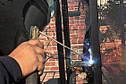
make - forge? - wedge for feathers-and-wedge rock-split
Hello all Setting the scene: "feathers" work well for splitting boulders so can...
Harbor Freight Tools' Quality
Any way to tell from a brand name which of the tools in Harbor Freight are...

Laser cutting
Has anyone had any parts laser cut? Is it expensive? I want to have some flat...

motor starndards outside NA
Motors all seem to follow NEMA sizes and standards in North America. What are...
ostrzenie noza
kuchennego. Temat niedawno byl, a ja sie ciagle nie dowiedzialem - czy po...

mini backhoe
I am trying to collect material and ideas in order to make a mini backhoe. I may...
UK users of disposable gas cylinders
I dont know if there's any UK users on here, but I would be interested to know...

WARNING: Metalworking Revisited - Deburring With Surface Conditioning Products - HARBOR FREIGHT SURPRISE
Off Topic Portion: The warning is for trolls like the one who replied once to...

Making Gear Cutters (Ivan Laws Book)
I've been reading Ivan Law's book on making gear cutters and he described the...

Making Molds On a POS Manual Mini Mill
I sold my first injection molds made on a tiny Taig CNC milling machine....

Cutting Silver with a plasma cutter?
I happened to be talking to a jeweler who was working on a large piece of 10 ga...

Plasma cutter settings
I can't help you with power settings. I'll be interested in those responses,...